






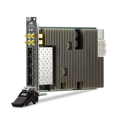

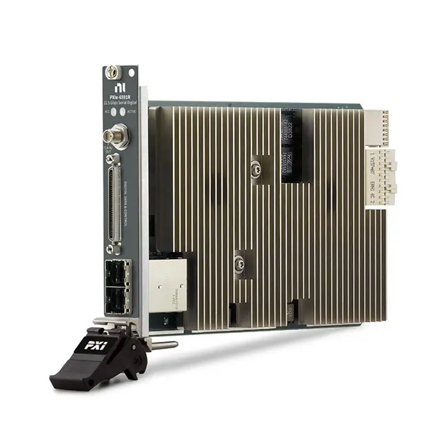
PXIe-6591 8-Channel 12.5 Gbps High-Speed Serial Instrument
The PXIe-6591, also identified as the PXIe-6591R in NI technical documentation, is an FPGA-based high-speed serial instrument designed for validating SerDes interfaces, implementing custom communication protocols and testing high-speed digital devices. It provides eight bidirectional serial lanes with line rates up to 12.5 Gbit/s per lane.
The instrument combines a Xilinx Kintex-7 FPGA, 2 GB of onboard DRAM, two Mini-SAS HD connectors and 20 auxiliary digital I/O lines. Its user-programmable architecture allows engineers to implement protocol-specific processing, custom triggering, data generation and real-time analysis directly in FPGA hardware.
The PXIe-6591 is part of the NI PXI high-speed serial instrument platform and is intended for automated validation, semiconductor testing, electronic system characterization and custom digital interface development.
PXIe-6591 Product Overview
Conventional serial instruments are typically limited to predefined protocols and fixed measurement functions. The PXIe-6591 uses a programmable FPGA architecture that enables engineers to define the serial protocol, data framing, triggering conditions and real-time processing required by a specific device under test.
The eight serial transceiver lanes are divided between two front-panel Mini-SAS HD connectors, with four transmit and receive lanes available on each connector. Copper and active optical Mini-SAS HD cables can be used to connect the instrument to development boards, custom fixtures and other high-speed serial equipment.
In addition to its serial transceivers, the PXIe-6591 provides 20 single-ended auxiliary digital I/O lines through a VHDCI connector. These lines can be used for device control, handshake signals, triggers, resets, status monitoring and communication with supporting test hardware.
Key Features of the PXIe-6591
Eight Bidirectional Serial Lanes
The PXIe-6591 provides eight high-speed transceiver lanes capable of transmitting and receiving data. Each lane can be configured according to the protocol and electrical requirements implemented in the FPGA design.
Maximum Line Rate of 12.5 Gbit/s
Each high-speed serial lane supports line rates from 500 Mbit/s to 8 Gbit/s and from 9.8 Gbit/s to 12.5 Gbit/s. Engineers should account for the unsupported range between 8 Gbit/s and 9.8 Gbit/s when selecting the module for a specific interface.
The published line rate represents the raw serial bit rate. Actual application payload throughput depends on protocol encoding, packet headers, error checking and other framing overhead.
Two Mini-SAS HD Ports
The front panel includes two Mini-SAS HD x4 connectors. Each port carries four high-speed transmit and receive lanes, providing a compact connection for all eight serial channels.
The Mini-SAS HD interface supports suitable copper and active optical cable assemblies, allowing the connection method to be selected according to cable length, signal-integrity requirements and the physical layout of the test system.
Xilinx Kintex-7 FPGA
The PXIe-6591 incorporates a Xilinx Kintex-7 XC7K410T FPGA. The FPGA can implement custom protocols, line encoding, packet generation, pattern checking, real-time data reduction and device-specific control logic.
- 254,200 lookup tables
- 508,400 flip-flops
- 1,540 DSP48 slices
- 28,620 kbit of block RAM
- User-programmable serial and digital processing logic
2 GB Onboard DRAM
The module includes 2 GB of onboard DRAM connected to the FPGA through a 512-bit interface. The memory can be used for waveform storage, burst data capture, packet buffering and temporary storage of high-speed test data.
Theoretical DRAM bandwidth is up to 10.5 GB/s, although usable performance depends on the FPGA design, memory access pattern and overall system configuration.
20 Auxiliary Digital I/O Lines
A VHDCI connector provides 20 single-ended auxiliary digital lines. These lines support data rates up to 200 Mbit/s and can be used to coordinate the serial measurement with control and status signals from the device under test.
Direction can be controlled on individual lines and changed on a cycle-by-cycle basis, enabling flexible bidirectional communication and hardware handshaking.
Flexible Reference Clocking
The PXIe-6591 supports serial transceiver reference clocks from 60 MHz to 700 MHz. Clock sources can include the PXI Express backplane, PXIe_DStarA or the front-panel SMA clock connection.
The front-panel SMA connector can support external clock input or clock output functions, depending on the FPGA configuration.
PXI Express Host Communication
The instrument uses a PCI Express Gen 2 x8 interface for communication with the host controller. It supports DMA transfers, interrupts and programmed I/O, with host streaming performance up to approximately 3.2 GB/s under supported system conditions.
PXIe-6591 Technical Specifications
| Product Model | PXIe-6591 / PXIe-6591R |
|---|---|
| NI Part Number | 783638-01 |
| Product Type | PXI High-Speed Serial Instrument |
| Serial Transceiver Lanes | 8 bidirectional TX/RX lanes |
| Serial Line-Rate Ranges | 500 Mbit/s to 8 Gbit/s and 9.8 Gbit/s to 12.5 Gbit/s |
| Maximum Line Rate | 12.5 Gbit/s per lane |
| Serial Connectors | 2 × Mini-SAS HD x4 |
| Lanes per Serial Connector | 4 |
| FPGA | Xilinx Kintex-7 XC7K410T |
| Onboard DRAM | 2 GB |
| DRAM Interface | 512-bit, 166 MHz |
| Theoretical DRAM Bandwidth | 10.5 GB/s |
| Auxiliary Digital I/O | 20 single-ended lines |
| Auxiliary DIO Data Rate | Up to 200 Mbit/s |
| Auxiliary DIO Connector | VHDCI |
| Reference Clock Range | 60 MHz to 700 MHz |
| External Clock Connector | 1 × SMA clock input/output |
| PXI Express Interface | PCI Express Gen 2 x8 |
| Host Streaming Performance | Up to approximately 3.2 GB/s |
| Operating Temperature | 0°C to 45°C |
| Programming Environment | LabVIEW FPGA |
| NI Lifecycle Status | Mature |
How the PXIe-6591 Works
The PXIe-6591 receives and transmits serial data through its FPGA-connected multigigabit transceivers. The FPGA can recover incoming data, identify frames, evaluate protocol conditions and transfer selected information to onboard memory or the host computer.
For generation applications, test patterns and protocol packets can be stored in onboard DRAM or generated algorithmically in the FPGA. The FPGA then formats and transmits the data through the selected serial lanes with deterministic hardware timing.
Measurement data can follow several processing paths:
- Immediate processing and response within the FPGA
- Temporary buffering in onboard DRAM
- DMA streaming to the PXI Express controller
- Conditional capture based on custom trigger logic
- Real-time comparison against expected protocol data
Programmable Serial Transceiver Technology
The high-speed serial transceivers use differential signaling with a nominal differential impedance of 100 Ω. Transmit amplitude, pre-emphasis, post-emphasis and receiver equalization can be adjusted through the FPGA design to improve signal quality for different channels and cable configurations.
Because the protocol logic is FPGA-based, the PXIe-6591 can be adapted to standard, proprietary and evolving serial interfaces. Final compatibility depends on the required line rate, encoding, clocking, electrical characteristics and available FPGA intellectual property.
Protocol Development and Validation
The PXIe-6591 can be used to develop custom serial endpoints, protocol-aware generators and real-time analyzers. Applications may include JESD204B development, Aurora-based communication, custom packet protocols and device-specific high-speed links.
NI has published example implementations for selected protocols, including JESD204B operation at rates up to 12.5 Gbit/s. These examples can provide a development starting point, but engineers should verify that the selected reference design supports the required device configuration and system architecture.
Typical PXIe-6591 Applications
- High-speed SerDes interface validation
- Custom serial protocol implementation
- JESD204B device testing
- Digital receiver and transmitter characterization
- Protocol packet generation and analysis
- Bit-error and pattern testing
- Semiconductor validation and production testing
- FPGA and ASIC interface testing
- Data converter interface validation
- High-speed embedded system testing
- Hardware-in-the-loop system development
- Automated functional testing
Software and FPGA Development
Users can develop PXIe-6591 applications with LabVIEW and the LabVIEW FPGA Module. The FPGA environment provides access to the serial transceivers, onboard DRAM, auxiliary digital I/O and PXI Express communication resources.
A typical system may require:
- A supported version of LabVIEW
- LabVIEW FPGA Module
- Applicable NI FlexRIO or high-speed serial instrument drivers
- Compatible Xilinx compilation tools
- A supported PXI Express chassis and embedded or remote controller
- Application-specific FPGA intellectual property or reference designs
Software and driver compatibility should be checked before selecting a PXIe-6591 for an existing test platform, particularly when maintaining systems built with older LabVIEW releases.
System Integration Requirements
A complete PXIe-6591 system normally includes the serial instrument, a compatible PXI Express chassis, a PXI controller or remote-control interface, Mini-SAS HD cables and any required device interface fixture.
System designers should evaluate the following requirements:
- Required serial line rate and protocol encoding
- Number of simultaneous transmit and receive lanes
- Reference-clock frequency and clock source
- Copper or optical cable requirements
- FPGA resource utilization
- Onboard buffering and host-streaming requirements
- Auxiliary control and trigger signals
- PXI Express chassis cooling and slot compatibility
- LabVIEW, driver and FPGA compiler compatibility
PXIe-6591 Troubleshooting Considerations
Serial Link Does Not Establish
Verify the configured line rate, reference clock, lane mapping, polarity, protocol encoding and transceiver settings. Confirm that the selected rate does not fall within the unsupported 8 Gbit/s to 9.8 Gbit/s range.
High Bit-Error Rate
Inspect the cable, adapter board, connector and PCB signal path. Transmitter emphasis and receiver equalization may need to be adjusted for the insertion loss and reflections of the channel.
Data Is Lost During Long Captures
Compare the incoming data rate with the available DRAM and host-transfer bandwidth. FPGA-based filtering, packet selection or data reduction may be necessary when the continuous input rate exceeds the sustainable host-streaming rate.
FPGA Compilation Fails
Confirm that the LabVIEW FPGA version, NI driver and Xilinx compilation tools support the PXIe-6591. Large designs may also require optimization to fit within the available FPGA logic, block RAM and timing constraints.
Auxiliary DIO Signals Are Incorrect
Verify the configured voltage standard, direction control and timing. Check the external connection carefully before enabling an auxiliary line as an output.
PXIe-6591 vs PXIe-6592
The PXIe-6591 is generally better suited to applications that need eight serial lanes and Mini-SAS HD connectivity. The PXIe-6592 provides four serial lanes through SFP+ connectors and supports line rates up to 10.3125 Gbit/s.
Both instruments use Kintex-7 FPGA technology, provide 2 GB of DRAM and support host streaming up to approximately 3.2 GB/s. Connector type, lane count, maximum rate and auxiliary I/O requirements are the primary selection factors.
PXIe-6591 vs PXIe-6593
The PXIe-6593 is a newer-generation eight-lane instrument with line rates up to 16.3 Gbit/s. It uses a Kintex UltraScale FPGA, provides 4 GB of DRAM and supports higher host-streaming performance.
The PXIe-6591 may remain appropriate for maintaining qualified systems that use Mini-SAS HD cabling and Kintex-7 FPGA code. The PXIe-6593 is generally more suitable when a new design requires higher bandwidth, newer FPGA resources or QSFP28 connectivity.
High-Speed Serial Instrument Comparison
| Model | Serial Lanes | Maximum Line Rate | FPGA Family | DRAM | Connector |
|---|---|---|---|---|---|
| PXIe-6591 | 8 | 12.5 Gbit/s | Kintex-7 | 2 GB | Mini-SAS HD |
| PXIe-6592 | 4 | 10.3125 Gbit/s | Kintex-7 | 2 GB | SFP+ |
| PXIe-6593 | 8 | 16.3 Gbit/s | Kintex UltraScale | 4 GB | QSFP28 |
| PXIe-6594 | 8 | 28.2 Gbit/s | Kintex UltraScale+ | 8 GB | QSFP28 |
| PXIe-7902 | 24 | 12.5 Gbit/s | Virtex-7 | 2 GB | Mini-SAS HD |
How to Select the Right Serial Instrument
Choose the PXIe-6591 when the application requires eight bidirectional lanes, line rates no higher than 12.5 Gbit/s, Mini-SAS HD connectivity and auxiliary digital control signals.
Consider a newer or higher-density instrument when:
- Line rates exceed 12.5 Gbit/s
- The design requires a newer UltraScale or UltraScale+ FPGA
- Host streaming above approximately 3.2 GB/s is required
- More than eight serial transceiver lanes are needed
- QSFP28 or another front-panel connector is preferred
- The equipment is being selected for a completely new long-term platform
The PXIe-6591 has reached NI Mature lifecycle status and is no longer recommended by NI for new designs. It remains relevant for repairing, expanding or duplicating systems already qualified around the PXIe-6591 or PXIe-6591R.
Recommended Related Products
- PXIe-6592 High-Speed Serial Instrument – Four-lane SFP+ alternative for serial applications up to 10.3125 Gbit/s.
- PXIe-6593 High-Speed Serial Instrument – Eight-lane, 16.3 Gbit/s platform with a newer FPGA and higher streaming bandwidth.
- PXIe-6594 High-Speed Serial Instrument – Eight-lane solution for applications requiring rates up to 28.2 Gbit/s.
- PXIe-7902 FPGA Module – 24-lane Mini-SAS HD platform for higher-density serial interfaces.
- PXIe-7903 FPGA Module – High-density, newer-generation platform with up to 48 serial transceiver lanes.
- PXIe-1085 Chassis – High-bandwidth PXI Express chassis for multichannel test systems.
- PXIe-8880 Embedded Controller – PXI Express controller for computationally demanding automated test applications.
Why Choose the PXIe-6591?
- Eight programmable bidirectional serial lanes
- Line rates up to 12.5 Gbit/s per lane
- Compact Mini-SAS HD connectivity
- User-programmable Kintex-7 FPGA
- 2 GB of onboard waveform and capture memory
- 20 auxiliary digital I/O lines
- Flexible external and PXI backplane clocking
- Suitable for custom and proprietary serial protocols
- Useful for maintaining existing PXIe-6591R test systems
Frequently Asked Questions
What is the PXIe-6591 used for?
The PXIe-6591 is used to generate, receive and analyze high-speed serial data. Common applications include SerDes validation, custom protocol development, JESD204B testing, semiconductor validation and automated device testing.
Are the PXIe-6591 and PXIe-6591R the same product?
Yes. NI currently lists the product as the PXIe-6591, while technical manuals, software examples and earlier documentation frequently use the PXIe-6591R designation.
How many serial lanes does the PXIe-6591 provide?
It provides eight bidirectional serial lanes. Four lanes are routed through each of the two Mini-SAS HD connectors.
What is the maximum serial rate?
The maximum raw serial line rate is 12.5 Gbit/s per lane. Supported ranges are 500 Mbit/s to 8 Gbit/s and 9.8 Gbit/s to 12.5 Gbit/s.
Does the PXIe-6591 support rates between 8 and 9.8 Gbit/s?
No. The documented operating ranges exclude serial line rates above 8 Gbit/s and below 9.8 Gbit/s.
Which FPGA does the PXIe-6591 use?
The module uses a Xilinx Kintex-7 XC7K410T FPGA.
How much onboard memory is available?
The PXIe-6591 provides 2 GB of onboard DRAM for data buffering, waveform storage and high-speed captures.
Does the module provide digital control lines?
Yes. It provides 20 single-ended auxiliary digital I/O lines through a VHDCI connector, with data rates up to 200 Mbit/s.
Which cables are required?
The serial ports require compatible Mini-SAS HD x4 copper or active optical cables. The auxiliary digital I/O connector requires an appropriate VHDCI cable or terminal accessory.
Can the PXIe-6591 implement proprietary protocols?
Yes. Its FPGA can be programmed to implement proprietary packet formats, triggering, data processing and control logic, provided the protocol fits within the module’s electrical, timing and FPGA resource limits.
Is the PXIe-6591 recommended for new designs?
NI classifies the PXIe-6591 as a Mature product and no longer recommends it for new designs. It is primarily suitable for supporting existing systems or applications that specifically require its Mini-SAS HD interface and established FPGA implementation.
What is the NI part number for the PXIe-6591?
The standard NI part number is 783638-01.
Request a Quote for the PXIe-6591
Contact us for current availability, condition, lead time and project pricing for the PXIe-6591 8-Channel High-Speed Serial Instrument. We can also help identify compatible PXI Express chassis, controllers, Mini-SAS HD cables and alternative high-speed serial modules for your test system.















