






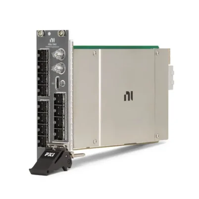
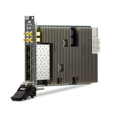

PXIe-7902 24-Lane 12.5 Gbps High-Speed Serial Instrument
The NI PXIe-7902 is an FPGA-based PXI Express high-speed serial instrument designed for SerDes validation, custom protocol implementation, real-time data processing and high-performance FPGA coprocessing. It provides 24 bidirectional TX/RX serial lanes, with each lane supporting line rates from 500 Mbit/s to 12.5 Gbit/s.
Built around a Xilinx Virtex-7 XC7VX485T FPGA, the PXIe-7902 allows engineers to implement application-specific high-speed serial interfaces using the LabVIEW FPGA Module and compatible FPGA IP. Six Mini-SAS HD x4 connectors provide access to the 24 multigigabit transceiver lanes.
The module also includes 2 GB of onboard DRAM and a PCI Express Gen 2 x8 host interface, supporting real-time signal processing, high-volume data movement and custom high-speed serial test applications.
PXIe-7902 Product Overview
The PXIe-7902 is designed for engineers who need more flexibility than a fixed-function serial protocol analyzer. Its FPGA can be programmed to implement custom framing, encoding, triggering, error detection, packet processing and protocol-specific logic directly in hardware.
The 24 serial lanes are arranged across six front-panel ports. Each Mini-SAS HD connector carries four transmit and four receive lanes, providing up to 50 Gbit/s of raw serial capacity per port when four lanes operate at 12.5 Gbit/s.
Actual payload throughput depends on the selected protocol, encoding overhead, FPGA implementation, reference-clock configuration and available host or DRAM bandwidth.
The standard NI part number for the PXIe-7902 is 784232-01. The product is currently classified by NI as a mature product and may not be recommended for new system designs, so lifecycle requirements should be reviewed before selection.
Key Features of the PXIe-7902
24 Bidirectional High-Speed Serial Lanes
The PXIe-7902 provides 24 transmit and receive lanes connected directly to the Virtex-7 FPGA multigigabit transceivers. Each lane can transmit and receive differential serial data.
Up to 12.5 Gbit/s Per Lane
Each serial lane supports rates from 500 Mbit/s to 8 Gbit/s and from 9.8 Gbit/s to 12.5 Gbit/s. There is a gap between 8 Gbit/s and 9.8 Gbit/s in the achievable line-rate range.
Six Mini-SAS HD x4 Ports
The front panel provides six Mini-SAS HD x4 connectors identified as Port 0 through Port 5. Each port contains four TX/RX transceiver lanes and can use compatible copper or active optical cables.
Xilinx Virtex-7 FPGA
The module includes a Xilinx Virtex-7 XC7VX485T FPGA with substantial logic, DSP and embedded-memory resources. It can perform custom protocol processing, data reduction, packet manipulation and real-time validation without relying entirely on the host controller.
2 GB Onboard DRAM
A 2 GB onboard DRAM bank supports waveform buffering, packet storage, lookup tables and FPGA processing. The memory has a theoretical maximum internal data rate of 10.5 GB/s.
FPGA Coprocessing
The PXIe-7902 can operate as a high-performance FPGA coprocessor for real-time algorithms. Data can be received through the serial ports, processed in the FPGA and transferred to DRAM, the host controller or another PXI module.
PCI Express Gen 2 x8 Interface
The module uses a PCI Express Gen 2 x8 PXI Express interface and supports host-streaming bandwidth up to approximately 3.2 GB/s under suitable system conditions.
Configurable Serial Protocols
The FPGA architecture supports custom and standards-based serial protocol implementations. Engineers can integrate compatible FPGA IP for encoding, link training, packet processing, error checking and protocol control.
Copper and Optical Cabling
The Mini-SAS HD ports support compatible electrical and active optical cables. Optical cabling can be useful for longer distances and systems requiring electrical isolation between equipment locations.
PXI Timing and Synchronization
The PXIe-7902 can use the PXI Express backplane reference clock, differential star timing resources and the front-panel CLK IN connection for FPGA and transceiver clocking.
PXIe-7902 Technical Specifications
| Product Model | NI PXIe-7902 |
|---|---|
| Part Number | 784232-01 |
| Product Type | FPGA-Based High-Speed Serial Instrument |
| Serial TX/RX Lanes | 24 bidirectional lanes |
| Number of Front-Panel Ports | 6 |
| Lanes per Port | 4 TX/RX lanes |
| Maximum Line Rate | 12.5 Gbit/s per lane |
| Supported Line-Rate Ranges | 500 Mbit/s to 8 Gbit/s and 9.8 Gbit/s to 12.5 Gbit/s |
| Front-Panel Serial Connectors | 6 × Mini-SAS HD x4 |
| Supported Cable Types | Electrical copper and active optical |
| Serial Signaling | AC-coupled differential |
| Differential Input Resistance | 100 Ω nominal |
| I/O Coupling Capacitor | 100 nF |
| FPGA | Xilinx Virtex-7 XC7VX485T |
| FPGA Package | FFG1158 |
| FPGA LUTs | 303,600 |
| FPGA Flip-Flops | 607,200 |
| DSP48 Slices | 2,800 |
| Embedded Block RAM | 37,080 kbit |
| Onboard DRAM | 2 GB, single bank |
| DRAM Theoretical Data Rate | 10.5 GB/s |
| PXI Express Interface | PCI Express Gen 2 x8 |
| Host Streaming Bandwidth | Up to approximately 3.2 GB/s |
| Data Transfer Methods | DMA, interrupts and programmed I/O |
| DMA Interrupt Channels | 32 |
| CLK IN Connector | SMA |
| CLK IN Frequency Range | 10 MHz to 300 MHz |
| Transceiver Reference Clock Range | 60 MHz to 700 MHz |
| Maximum Backplane Power | 38.25 W |
| Operating Temperature | 0°C to 55°C |
| Software | LabVIEW FPGA Module and NI High-Speed Serial Instrument support |
Understanding the 24-Lane Architecture
The PXIe-7902 provides six Mini-SAS HD ports, with four high-speed serial lanes assigned to each port:
- Port 0: 4 TX/RX lanes
- Port 1: 4 TX/RX lanes
- Port 2: 4 TX/RX lanes
- Port 3: 4 TX/RX lanes
- Port 4: 4 TX/RX lanes
- Port 5: 4 TX/RX lanes
At the maximum 12.5 Gbit/s line rate, one four-lane port represents up to 50 Gbit/s of raw serial capacity in each direction. Across all 24 lanes, the theoretical aggregate serial capacity is substantially higher than the PXI host interface bandwidth.
For this reason, many applications process, filter, compare or reduce serial data inside the FPGA before transferring the required results to the host.
How the PXIe-7902 Works
Incoming serial data passes through the Mini-SAS HD connectors and reaches the Virtex-7 GTX multigigabit transceivers. The transceivers recover serial data and clocks before passing parallelized data into the FPGA fabric.
Custom FPGA logic can then perform functions such as:
- Line encoding and decoding
- Frame and packet detection
- Protocol state-machine control
- Error detection and counting
- Data filtering and reduction
- Packet modification or retransmission
- Real-time triggering
- Data buffering in onboard DRAM
Processed data can be transferred to the host controller through DMA or directed to another serial port. This FPGA-based architecture provides deterministic operation and low latency.
FPGA Resources and Real-Time Processing
The Virtex-7 XC7VX485T provides 303,600 lookup tables, 607,200 flip-flops, 2,800 DSP48 slices and approximately 37 Mbit of embedded block RAM.
These resources allow developers to implement multiple high-speed serial interfaces together with real-time processing functions. DSP slices can be used for mathematical operations, while block RAM can support packet buffers, state tables and intermediate processing data.
The FPGA design must remain within the available logic, routing, timing, power and transceiver resources. Large multi-protocol designs may require careful clock-domain management and FPGA timing optimization.
Onboard DRAM
The PXIe-7902 includes 2 GB of onboard DRAM connected directly to the FPGA. It can store significantly more data than the FPGA’s embedded block RAM.
Typical DRAM uses include:
- High-speed packet buffering
- Temporary serial data capture
- Replay-pattern storage
- Lookup tables
- Protocol transaction queues
- Data buffering between clock domains
The theoretical DRAM data rate is 10.5 GB/s, although practical performance depends on the FPGA memory-controller design and access pattern.
Host Streaming and DMA
The PCI Express Gen 2 x8 interface supports high-speed transfers between the FPGA and PXI controller. NI specifies host-streaming performance up to approximately 3.2 GB/s for the PXIe-7902 under suitable system conditions.
Because the combined capacity of the 24 serial lanes is much greater than the host interface bandwidth, applications that operate many lanes simultaneously usually need FPGA-based filtering, protocol processing or data reduction.
DMA channels can transfer data between FPGA memory and the host without requiring the processor to manage every transaction.
Clocking and Reference Sources
Stable reference clocks are essential for multigigabit serial operation. The PXIe-7902 supports several timing resources:
- Front-panel SMA CLK IN
- PXIe_CLK100 backplane reference
- PXIe_DStarA differential star clock
- Internal multigigabit transceiver reference-clock generation
The CLK IN connector accepts frequencies from 10 MHz to 300 MHz. The programmable multigigabit transceiver reference-clock generator covers approximately 60 MHz to 700 MHz.
The selected reference clock must meet the requirements of the implemented serial protocol and FPGA transceiver configuration.
Mini-SAS HD Connectivity
The PXIe-7902 uses six Mini-SAS HD x4 connectors for high-density serial connectivity. These connectors allow four TX/RX lanes to be carried through each cable assembly.
Compatible cable options include:
- Mini-SAS HD x4 copper cable
- Mini-SAS HD x4 active optical cable
- Custom breakout assemblies designed for the target interface
Cable selection should consider length, signal loss, insertion loss, connector mapping, polarity and the required serial line rate.
Copper vs Active Optical Cables
Copper Cables
Copper Mini-SAS HD cables are practical for short connections within a rack or laboratory setup. They do not require optical conversion but may experience greater insertion loss as length and frequency increase.
Active Optical Cables
Active optical cables support longer connection distances and can reduce susceptibility to electromagnetic interference. The PXIe-7902 can provide 3.3 V optical-cable power through each compatible port.
Confirm cable compatibility and pin mapping before connecting any optical or custom cable assembly.
Custom Serial Protocol Implementation
The PXIe-7902 is not limited to one fixed serial standard. Engineers can integrate compatible protocol IP or develop custom FPGA logic for proprietary interfaces.
Potential protocol functions include:
- Serializer/deserializer control
- Comma and alignment-character detection
- 8b/10b or other line encoding
- Link initialization and training
- Packet framing and deframing
- Cyclic redundancy checking
- Error injection and error counting
- Loopback and retransmission
Protocol support is determined by the FPGA design, transceiver capabilities and available IP. The PXIe-7902 does not automatically provide every serial protocol without the required FPGA implementation.
Typical PXIe-7902 Applications
- SerDes interface validation
- High-speed serial protocol testing
- Custom protocol implementation
- Real-time data transmission and reception
- Bit-error and link-integrity testing
- Semiconductor functional testing
- FPGA and ASIC validation
- Packet processing and inspection
- High-speed data recording and replay
- Digital video and communication interfaces
- High-performance embedded systems
- FPGA-based data reduction
- Automated production test
- Aerospace and defense communication testing
Semiconductor and SerDes Validation
The PXIe-7902 can generate and receive multigigabit serial traffic for validating the digital interfaces of FPGAs, ASICs and communication devices.
Custom FPGA logic can perform link initialization, packet generation, error injection and error counting in real time. The module can also be synchronized with power supplies, oscilloscopes and other instruments to correlate link behavior with voltage, timing and environmental conditions.
FPGA Coprocessing Applications
In addition to serial protocol testing, the PXIe-7902 can be used as an FPGA coprocessor. Data can enter through the PXI Express interface or serial ports, be processed in real time and then be stored, retransmitted or returned to the host.
Potential FPGA-coprocessing functions include:
- Real-time filtering
- Data compression and reduction
- Packet classification
- Low-latency decision logic
- Inline format conversion
- High-speed triggering
PXIe-7902 Software Support
The PXIe-7902 is programmed using the LabVIEW FPGA Module together with NI support for high-speed serial instruments. Developers can create custom FPGA personalities and host applications for configuration, monitoring and data transfer.
Development resources may include:
- LabVIEW FPGA Module
- NI High-Speed Serial Instrument support
- LabVIEW Instrument Design Libraries
- Socketed Component-Level IP
- Compatible Xilinx protocol IP
- VHDL integration
- LabVIEW host applications
Development of a new serial protocol requires FPGA and high-speed digital design experience. Existing sample projects or protocol IP can reduce development time when they meet the application requirements.
PXIe-7902 System Requirements
A complete PXIe-7902 system normally requires:
- A compatible PXI Express chassis
- An embedded PXI controller or external computer interface
- A PXI Express slot with suitable link width and cooling
- LabVIEW and the LabVIEW FPGA Module
- NI High-Speed Serial Instrument software support
- Compatible FPGA compilation tools
- Mini-SAS HD copper or optical cables
- Appropriate serial protocol IP or custom FPGA logic
The module can operate in x1, x4, x8 and x16 PXI Express or hybrid-compatible slots, but the available host bandwidth depends on the slot’s PCI Express link width.
Cooling and Installation Considerations
The PXIe-7902 can draw up to 38.25 W from the PXI Express backplane depending on the FPGA design. High transceiver utilization and complex FPGA processing can increase power consumption and heat generation.
For reliable operation:
- Use a chassis with sufficient slot cooling capacity
- Set the chassis fan mode as required by the specifications
- Install slot blockers and filler panels in unused positions
- Keep chassis air inlets and outlets unobstructed
- Allow the specified warm-up period before critical operation
PXIe-7902 vs PXIe-7903
| Specification | PXIe-7902 | PXIe-7903 |
|---|---|---|
| Maximum Line Rate | 12.5 Gbit/s | 28.2 Gbit/s |
| TX/RX Lanes | 24 | 48 |
| FPGA | Virtex-7 XC7VX485T | Virtex UltraScale+ XCVU11P |
| Onboard DRAM | 2 GB | 20 GB |
| Host Streaming Bandwidth | Approximately 3.2 GB/s | Up to approximately 7 GB/s |
| Module Width | Single slot | Two slots |
| Product Generation | Mature Virtex-7 platform | Newer UltraScale+ platform |
The PXIe-7903 is the recommended higher-performance option for new applications requiring more lanes, higher line rates, additional FPGA resources or greater onboard memory.
Comparison with Related High-Speed Serial Instruments
| Model | TX/RX Lanes | Maximum Line Rate | FPGA | Connector |
|---|---|---|---|---|
| PXIe-6591R | 8 | 12.5 Gbit/s | Kintex-7 K410T | Mini-SAS HD |
| PXIe-6592R | 4 | 10.3125 Gbit/s | Kintex-7 K410T | SFP+ |
| PXIe-7902 | 24 | 12.5 Gbit/s | Virtex-7 XC7VX485T | Mini-SAS HD |
| PXIe-6593 | 8 | 16.3 Gbit/s | Kintex UltraScale | QSFP28 |
| PXIe-6594 | 8 | 28.2 Gbit/s | Kintex UltraScale+ | QSFP28 |
| PXIe-7903 | 48 | 28.2 Gbit/s | Virtex UltraScale+ | Mini-SAS HD |
Recommended Related Products
- PXIe-7903 – newer 48-lane high-speed serial FPGA instrument with line rates up to 28.2 Gbit/s.
- PXIe-6591R – 8-lane, 12.5 Gbit/s FPGA-based serial instrument with Mini-SAS HD connectivity.
- PXIe-6592R – 4-lane high-speed serial instrument with SFP+ connections.
- PXIe-6593 – 8-lane Kintex UltraScale serial instrument supporting up to 16.3 Gbit/s.
- PXIe-6594 – 8-lane, 28.2 Gbit/s UltraScale+ serial instrument with QSFP28 connectors.
- PXIe-1085 – high-bandwidth PXI Express chassis for FPGA and high-speed serial systems.
- PXIe-8880 – embedded PXI controller for high-performance automated test applications.
PXIe-7902 Selection Guidance
Before selecting the PXIe-7902, confirm that:
- No more than 24 TX/RX serial lanes are required
- The required line rate is within the supported ranges
- The application can use Mini-SAS HD x4 connectivity
- The Virtex-7 FPGA provides sufficient logic and DSP resources
- 2 GB of onboard DRAM is sufficient
- The host-streaming requirement does not exceed the practical PXI interface bandwidth
- Suitable protocol IP or FPGA development resources are available
- The chassis provides adequate PCI Express bandwidth and cooling
- The mature product lifecycle is acceptable for the project
Common Troubleshooting Checks
The PXIe-7902 Is Not Detected
Confirm that the module is fully installed in a compatible PXI Express slot and that the required NI high-speed serial support software is installed. Use NI MAX to verify chassis and module recognition.
The FPGA Compilation Fails
Verify software and compilation-tool compatibility. Check FPGA resource usage, clock constraints, transceiver placement, CLIP configuration and protocol IP requirements.
The Serial Link Does Not Establish
Confirm the reference-clock frequency, serial line rate, cable mapping, lane polarity, encoding and protocol initialization sequence. Verify that the far-end device uses compatible electrical and protocol settings.
Bit Errors Occur at High Line Rates
Inspect the cable length, insertion loss, connector quality and reference-clock jitter. Adjust transmitter amplitude, pre-emphasis and receiver equalization where supported by the FPGA transceiver configuration.
Host Streaming Cannot Sustain the Data Rate
Compare the combined serial payload with the practical host-streaming limit. Use FPGA processing, filtering or data reduction to decrease the amount of data transferred to the controller.
The Module Becomes Too Hot
Confirm that the chassis provides sufficient cooling, the fan mode is configured correctly and unused slots contain appropriate filler panels. Reduce FPGA resource or transceiver activity if the design exceeds the available power and thermal budget.
Frequently Asked Questions
What is the PXIe-7902 used for?
The PXIe-7902 is used for high-speed serial protocol testing, SerDes validation, real-time data processing and FPGA coprocessing.
How many serial lanes does the PXIe-7902 provide?
It provides 24 bidirectional TX/RX serial lanes arranged across six Mini-SAS HD x4 ports.
What is the maximum data rate?
The maximum line rate is 12.5 Gbit/s per serial lane.
Are all rates between 500 Mbit/s and 12.5 Gbit/s supported?
No. The supported ranges are 500 Mbit/s to 8 Gbit/s and 9.8 Gbit/s to 12.5 Gbit/s.
Which FPGA does the PXIe-7902 use?
It uses a Xilinx Virtex-7 XC7VX485T FPGA.
How much onboard memory is available?
The module includes 2 GB of onboard DRAM in addition to the FPGA’s embedded block RAM.
Which connectors does the PXIe-7902 use?
It provides six Mini-SAS HD x4 serial connectors and one SMA CLK IN connector.
Does the PXIe-7902 support optical cables?
Yes. It supports compatible Mini-SAS HD electrical and active optical cables.
Can the PXIe-7902 test any serial protocol?
It can support many standards-based and custom protocols, but the appropriate FPGA IP and application logic must be implemented. Protocol support is not automatic.
Which software is required?
Development typically requires LabVIEW, the LabVIEW FPGA Module and NI support software for high-speed serial instruments.
What is the PXIe-7902 part number?
The standard NI part number is 784232-01.
Can the PXIe-7902 operate independently?
No. It requires a compatible PXI Express chassis and an embedded controller or external computer connection.
Is the PXIe-7902 recommended for new designs?
NI currently identifies the PXIe-7902 as a mature product. New designs should also evaluate the PXIe-7903 and other current high-speed serial instruments.
Why Choose the PXIe-7902?
The PXIe-7902 is well suited to systems requiring a large number of FPGA-connected serial lanes in a single PXI Express slot. Its 24 TX/RX lanes, 12.5 Gbit/s line rate, Virtex-7 FPGA and 2 GB DRAM support demanding custom protocol and real-time processing applications.
For existing PXIe-7902 systems, replacement units can help maintain validated test configurations without redesigning FPGA code, cabling and fixtures around a newer platform.
Request a Quote for the PXIe-7902
Contact us for current availability, lead time and project pricing for the NI PXIe-7902 High-Speed Serial Instrument, part number 784232-01.
We can also help identify compatible PXI Express chassis, controllers, Mini-SAS HD cables and alternative high-speed serial instruments for new or existing test systems.















