






PXIe-5641 Reconfigurable Intermediate-Frequency Transceiver
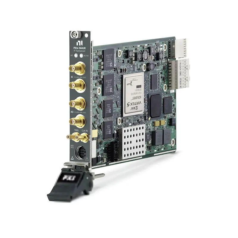
The PXIe-5641, also documented as the PXIe-5641R, is a reconfigurable intermediate-frequency transceiver with two analog input channels and two analog output channels. It is designed for real-time spectrum analysis, software-defined radio, RFID testing and custom RF signal-processing applications.
The module combines 14-bit ADCs and DACs with a user-programmable Xilinx Virtex-5 SX95T FPGA. It supports IF signals through 80 MHz, input sampling up to 100 MS/s, output sampling up to 200 MS/s and direct hardware processing with low latency.
Key Features of the PXIe-5641
- Two intermediate-frequency input channels
- Two intermediate-frequency output channels
- 14-bit analog-to-digital converters
- 14-bit digital-to-analog converters
- Input sampling rates from 30 MS/s to 100 MS/s
- Output sampling rates from 30 MS/s to 200 MS/s
- 250 kHz to 80 MHz characterized IF passband
- 20 MHz maximum instantaneous input bandwidth
- Up to 40 MHz digital modulation bandwidth
- Xilinx Virtex-5 SX95T FPGA
- 128 MB onboard DRAM
- Seven configurable auxiliary digital I/O lines
- External reference and sample clock support
- Peer-to-peer data streaming support
- Single-slot PXI Express module
PXIe-5641 Technical Specifications
| Product Model | PXIe-5641 / PXIe-5641R |
|---|---|
| Part Number | 780710-01 |
| Product Type | Reconfigurable PXI IF Transceiver |
| Input Channels | 2 |
| Output Channels | 2 |
| IF Frequency Range | Up to 80 MHz |
| Characterized Passband | 250 kHz to 80 MHz |
| Input ADC Resolution | 14 bits |
| Input Sampling Rate | 30 MS/s to 100 MS/s |
| Maximum Input Bandwidth | 20 MHz |
| Input Full-Scale Level | +8.5 dBm peak at 10 MHz, typical |
| Maximum Input Without Damage | +24 dBm peak |
| Output DAC Resolution | 14 bits |
| Output Sampling Rate | 30 MS/s to 200 MS/s |
| Maximum Modulation Bandwidth | 40 MHz |
| Maximum Output Power | Up to +2 dBm with compensation filters disabled |
| Input and Output Impedance | 50 Ω nominal |
| Input and Output Coupling | AC |
| FPGA | Xilinx Virtex-5 SX95T |
| Onboard DRAM | 128 MB |
| Internal Timebase | 200 MHz |
| Auxiliary Digital I/O | 7 configurable lines |
| Peer-to-Peer Streaming | Supported |
| Bus Interface | PXI Express |
| Module Size | 3U, single slot |
Part Number and Configuration
| Part Number | Analog I/O | FPGA | Onboard Memory | Bus |
|---|---|---|---|---|
| 780710-01 | 2 IF inputs and 2 IF outputs | Virtex-5 SX95T | 128 MB DRAM | PXI Express |
Dual IF Input Channels
The PXIe-5641 provides two AC-coupled, 50 Ω IF input channels. Each channel uses a 14-bit ADC and supports sampling rates between 30 MS/s and 100 MS/s.
The inputs can be used for simultaneous acquisition of two IF signals, I/Q signal pairs or separate receiver paths. The maximum instantaneous input bandwidth is 20 MHz when using the onboard digital downconverter.
Dual IF Output Channels
Two 14-bit DAC channels generate AC-coupled IF signals at sampling rates from 30 MS/s to 200 MS/s. Each output includes a digital upconverter with interpolation, digital mixing and numerically controlled oscillator functions.
The digital upconverter supports modulation bandwidths up to 40 MHz. Pulse-shaping filters required by a specific communication standard must be implemented in the FPGA application or signal-generation software.
Virtex-5 FPGA Processing
The PXIe-5641 includes a user-programmable Xilinx Virtex-5 SX95T FPGA. It provides 94,208 logic cells, 640 DSP blocks and up to 8,784 kbits of block RAM for real-time signal-processing functions.
Engineers can implement digital downconversion, filtering, triggering, modulation, demodulation, spectrum processing and custom decision logic directly in hardware. FPGA execution provides deterministic timing and low-latency responses that are difficult to achieve with host software alone.
128 MB Onboard DRAM
The module includes 128 MB of onboard DRAM with a theoretical maximum data rate of 1,600 MB/s. This memory can be used for waveform storage, acquisition buffering and FPGA-based signal processing.
Onboard memory is useful when the application must capture transient signals before transferring data to the controller or continuously generate stored IF waveforms.
Digital Downconversion and Signal Acquisition
The input subsystem can digitally translate a selected IF band to complex baseband data. Digital filtering and decimation reduce the data rate while preserving the signal bandwidth required by the application.
This architecture supports applications such as real-time spectral monitoring, custom demodulation and channelized receivers. FPGA code can also respond immediately when a signal meets a defined frequency, amplitude or timing condition.
Digital Upconversion and Modulation
Each output DAC has an associated digital upconverter that can translate complex baseband data to an IF carrier. Supported interpolation factors range from 4× to 252×.
The numerically controlled oscillator provides fine tuning resolution for custom waveform generation. Engineers can develop proprietary modulation schemes or reproduce recorded IF signals without relying on a fixed-function signal generator.
Clocking and Synchronization
The PXIe-5641 uses a calibrated 200 MHz internal timebase. Its CLK IN connector can accept an external reference clock from 1 MHz to 100 MHz in 1 MHz increments or an external sample clock from 30 MHz to 200 MHz.
External clocking and PXI trigger resources allow the module to synchronize with RF upconverters, downconverters, digitizers and other modular instruments. This is important for phase-coherent and multichannel measurement systems.
Trigger and Auxiliary Digital I/O
The module includes an SMB trigger connector and seven configurable auxiliary digital lines. The digital lines can implement custom handshaking, status monitoring, triggering and control interfaces.
Triggering can be initiated through software, the external trigger connection or PXI trigger lines when using a LabVIEW FPGA application. Trigger polarity and response behavior can be customized in FPGA hardware.
Peer-to-Peer Data Streaming
Peer-to-peer streaming allows the PXIe-5641 to transfer data directly to compatible PXI Express modules without routing every transfer through the host controller.
This can reduce host CPU usage and latency in systems that combine the IF transceiver with FPGA coprocessors, digitizers or other real-time processing modules.
Typical PXIe-5641 Applications
- Software-defined radio development
- RFID reader and tag testing
- Real-time spectrum analysis
- Spectral monitoring
- Custom modulation and demodulation
- Digital radio research
- IF waveform acquisition and generation
- Receiver and transmitter prototyping
- RF dynamic testing
- Signal intelligence research
- Hardware-in-the-loop RF simulation
- Custom communication protocol testing
Software and Driver Support
The PXIe-5641 can be programmed using the NI-5640R instrument driver or the LabVIEW FPGA Module. The instrument driver provides a higher-level interface for standard acquisition and generation, while LabVIEW FPGA provides direct access to reconfigurable processing resources.
Software selection depends on whether the application requires conventional IF transceiver functions or a custom FPGA personality. Verify compatibility among the driver, LabVIEW version, FPGA compilation tools, controller and operating system.
Front-Panel Connections
| Connector | Type | Function |
|---|---|---|
| AI CH 0 and AI CH 1 | SMA | 50 Ω analog IF inputs |
| AO CH 0 and AO CH 1 | SMA | 50 Ω analog IF outputs |
| CLK IN | SMB | External reference or sample clock input |
| TRIG | SMB | External trigger connection |
| DIO / AUX I/O | 9-pin mini-DIN | Seven configurable digital I/O lines |
PXI Chassis and System Integration
The PXIe-5641 is a single-slot PXI Express module requiring a compatible PXI Express chassis and controller. The chassis fan should be configured for high-speed operation when required to maintain specified performance.
Compatible chassis options include the PXIe-1092, PXIe-1085 and other NI PXI Express chassis with sufficient cooling, power and data bandwidth.
Installation and Troubleshooting
Module Is Not Detected
Confirm that the PXIe-5641 is fully installed in a compatible PXI Express peripheral slot. Check chassis communication and install the NI-5640R driver or required RIO software before reviewing the device in NI Measurement & Automation Explorer.
No Input Signal Is Detected
Verify the input frequency, signal level, selected input channel and digital downconverter configuration. The inputs are AC-coupled, and their characterized passband begins at approximately 250 kHz.
Output Signal Level Is Lower Than Expected
Check whether CIC and inverse-sinc compensation are enabled. The typical full-scale output is approximately −4 dBm with default compensation enabled and can reach approximately +2 dBm with the compensation filters disabled.
FPGA Bitfile Cannot Be Downloaded
Confirm that the FPGA application was compiled specifically for the PXIe-5641R target. Verify that the required LabVIEW FPGA and NI-RIO versions are installed.
Samples Are Lost During Continuous Acquisition
Reduce the data rate through FPGA filtering or decimation, increase host-side buffering and verify the available PXI Express bandwidth. Peer-to-peer streaming may be appropriate when data must be sent directly to another compatible module.
Channels Are Not Synchronized
Confirm that both channels use the intended clock source and start trigger. For multiple modules, distribute a common reference clock and use PXI trigger resources to coordinate acquisition and generation.
PXIe-5641 Comparison with Related RF Instruments
| Model | Primary Function | Recommended Selection |
|---|---|---|
| PXIe-5641 | Dual-input, dual-output reconfigurable IF transceiver | Custom FPGA-based IF acquisition and generation |
| PXIe-5820 | Baseband vector signal transceiver | Wider-bandwidth baseband and direct I/Q applications |
| PXIe-5841 | RF vector signal transceiver | Integrated RF signal generation and analysis |
| PXIe-5668 | Vector signal analyzer | High-performance RF spectrum and modulation analysis |
| PXIe-5673 | Vector signal generator | Standard RF waveform generation |
Recommended Related Products
- PXIe-5820 Baseband Vector Signal Transceiver – suitable for high-bandwidth baseband and direct I/Q testing
- PXIe-5841 Vector Signal Transceiver – combines RF signal generation and analysis in one instrument
- PXIe-5668 Vector Signal Analyzer – supports spectrum and modulation measurements
- PXIe-5673 Vector Signal Generator – provides modulated RF signal generation
- PXIe-1092 PXI Express Chassis – provides a platform for synchronized RF and IF test systems
Additional compatible RF hardware is available in our NI PXI modules category.
How to Select the PXIe-5641
Choose the PXIe-5641 when an application requires simultaneous dual-channel IF acquisition and generation with custom FPGA processing. It is especially useful for proprietary communications, real-time spectrum processing and software-defined radio development.
Before purchasing, confirm the IF frequency, bandwidth, signal level, channel count, sampling rate, FPGA capacity, driver support, clocking requirements and PXI Express chassis compatibility.
Why Choose the PXIe-5641?
The PXIe-5641 combines dual IF inputs, dual IF outputs, 14-bit converters and a programmable FPGA in a compact PXI Express module. Its open processing architecture supports specialized acquisition, generation and real-time RF algorithms that cannot be implemented with conventional fixed-function instruments.
Frequently Asked Questions
How many input and output channels does the PXIe-5641 provide?
The PXIe-5641 provides two 14-bit IF input channels and two 14-bit IF output channels.
What is the maximum IF frequency?
The module supports IF signals through 80 MHz. Its characterized analog passband extends from approximately 250 kHz to 80 MHz because the inputs and outputs are AC-coupled.
What are the maximum sampling rates?
The analog inputs sample at rates up to 100 MS/s, while the analog outputs operate at rates up to 200 MS/s.
Which FPGA does the PXIe-5641 use?
The module uses a Xilinx Virtex-5 SX95T FPGA with 94,208 logic cells and 640 DSP blocks.
Does the PXIe-5641 include onboard memory?
Yes. It includes 128 MB of onboard DRAM for acquisition buffering, waveform storage and FPGA processing.
Can the PXIe-5641 generate RF signals directly?
The PXIe-5641 is an IF transceiver operating through 80 MHz. Higher-frequency RF operation requires external frequency conversion or a vector signal transceiver designed for direct RF generation and analysis.
Can the PXIe-5641 be programmed with LabVIEW FPGA?
Yes. It can be programmed using LabVIEW FPGA for custom processing or operated through the NI-5640R instrument driver.
What is the part number for the PXIe-5641?
The standard NI part number for the PXIe-5641 is 780710-01.
Request a Quote for the PXIe-5641
Contact us for current availability, lead time and project pricing for the PXIe-5641 Reconfigurable IF Transceiver. We can also help identify compatible PXI chassis, controllers, RF conversion modules, cables and software for your test system.















