






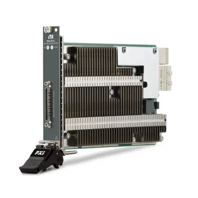
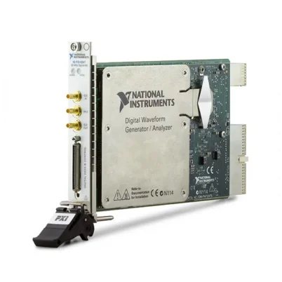

PXIe-6569 64-Channel LVDS FlexRIO Digital I/O Module
The PXIe-6569 is a high-density FlexRIO digital I/O module featuring up to 64 LVDS channels, a maximum line rate of 1.25 Gbit/s and a user-programmable Xilinx Kintex UltraScale FPGA. It is designed for real-time digital interfacing, custom protocol implementation and high-speed electronic device validation.
Multiple hardware configurations are available with 64 LVDS inputs, 64 LVDS outputs or 32 LVDS inputs and 32 LVDS outputs. Each version also provides eight bidirectional single-ended PFI channels and two bidirectional differential PFI channels for clocking, triggering and device control.
The PXIe-6569 integrates FPGA processing, high-speed digital I/O and onboard DRAM in a single PXI Express module, enabling deterministic processing without continuously transferring all data to the host computer.
PXIe-6569 Product Overview
The PXIe-6569 is intended for engineers who need more flexibility than a fixed-function digital instrument can provide. Its FPGA can implement application-specific timing, data framing, encoding, decoding, pattern generation and real-time response logic.
The LVDS channels support data rates up to 1.25 Gbit/s per line and use 100 Ω differential termination. A high-density Samtec SEARAY connector provides access to the LVDS, PFI and ground signals.
Customers can select either a Kintex UltraScale KU035 or KU060 FPGA. KU035 versions provide 2 GB of onboard DRAM, while KU060 versions provide 4 GB for applications requiring additional FPGA resources and data-buffering capacity.
Key Features of the PXIe-6569
Up to 64 LVDS Channels
The PXIe-6569 is available in three digital channel configurations:
- 64 LVDS input channels
- 64 LVDS output channels
- 32 LVDS input and 32 LVDS output channels
The LVDS channels have fixed directions according to the selected hardware variant. Customers should confirm whether the application requires acquisition, generation or simultaneous input and output before selecting a part number.
1.25 Gbit/s Maximum LVDS Line Rate
Each LVDS channel supports line rates up to 1.25 Gbit/s. The high channel density and per-line speed make the module suitable for wide parallel interfaces, data converter connections, proprietary digital buses and real-time hardware emulation.
Kintex UltraScale FPGA
The user-programmable FPGA provides direct access to the digital I/O, timing resources and onboard memory. It can perform deterministic operations such as:
- Custom protocol encoding and decoding
- Digital waveform generation and acquisition
- Real-time packet inspection
- Trigger detection and event response
- Data reduction and filtering
- Custom handshaking and control
- Parallel-to-serial and serial-to-parallel conversion
KU035 and KU060 FPGA Options
The KU035 configuration is suitable for many custom digital interfacing applications and includes 2 GB of DRAM. The KU060 configuration provides more FPGA resources and 4 GB of DRAM for larger protocol implementations, deeper buffering and more complex real-time processing.
Eight Bidirectional Single-Ended PFI Channels
Eight single-ended PFI channels support individually controlled input or output operation. Supported voltage families include 1.2 V, 1.5 V, 1.8 V, 2.5 V and 3.3 V.
The maximum data rate depends on the selected voltage family:
- Up to 300 Mbit/s at 3.3 V, 2.5 V or 1.8 V
- Up to 280 Mbit/s at 1.5 V
- Up to 240 Mbit/s at 1.2 V
Two Differential PFI Channels
The module provides two bidirectional differential PFI channels with maximum line rates up to 300 Mbit/s. These lines can be used for auxiliary clocks, triggers, synchronization or application-specific control signals.
High-Bandwidth Onboard DRAM
Two independent DRAM banks provide temporary storage for generated and acquired data. The memory subsystem has a maximum theoretical aggregate data rate of 17 GB/s, with up to 8.5 GB/s available per bank.
Flexible Clocking and Synchronization
The PXIe-6569 supports an internal sample clock, the PXI 10 MHz reference clock and an external 10 MHz reference clock. A front-panel connection can also provide an external sample or reference clock output.
NI-TClk can synchronize digital outputs across multiple identical PXIe-6569 modules with sample-level alignment. This TClk synchronization function applies to digital outputs and does not support synchronization of the digital input channels.
PXIe-6569 Part Number Configurations
| Part Number | LVDS Configuration | FPGA | Onboard DRAM |
|---|---|---|---|
| 787280-01 | 32 inputs and 32 outputs | Kintex UltraScale KU035 | 2 GB |
| 787283-01 | 32 inputs and 32 outputs | Kintex UltraScale KU060 | 4 GB |
| 787285-01 | 64 inputs | Kintex UltraScale KU035 | 2 GB |
| 787282-01 | 64 inputs | Kintex UltraScale KU060 | 4 GB |
| 787284-01 | 64 outputs | Kintex UltraScale KU035 | 2 GB |
| 787281-01 | 64 outputs | Kintex UltraScale KU060 | 4 GB |
PXIe-6569 Technical Specifications
| Product Model | PXIe-6569 |
|---|---|
| Product Type | FlexRIO Digital I/O Module |
| Bus Interface | PXI Express |
| LVDS Channel Configurations | 64 input, 64 output, or 32 input and 32 output |
| Maximum LVDS Line Rate | 1.25 Gbit/s per channel |
| LVDS Input Termination | 100 Ω |
| LVDS Output Impedance | 100 Ω |
| Single-Ended PFI Channels | 8 bidirectional channels |
| Single-Ended Logic Families | 1.2 V, 1.5 V, 1.8 V, 2.5 V and 3.3 V |
| Single-Ended Maximum Data Rate | Up to 300 Mbit/s, depending on voltage family |
| Differential PFI Channels | 2 bidirectional channels |
| Differential PFI Maximum Rate | 300 Mbit/s |
| FPGA Options | Xilinx Kintex UltraScale KU035 or KU060 |
| Onboard DRAM | 2 GB with KU035; 4 GB with KU060 |
| DRAM Banks | 2 |
| Theoretical DRAM Data Rate | 17 GB/s aggregate |
| Digital I/O Connector | Samtec SEARAY |
| External Reference Clock Input | 1 |
| Operating Temperature | 0°C to 55°C |
| Maximum Power | 58 W, FPGA design dependent |
| Programming Environment | LabVIEW FPGA |
| Lifecycle Status | Active |
How the PXIe-6569 Works
Digital signals are routed from the Samtec SEARAY connector directly to the LVDS and PFI interface circuitry connected to the FPGA. The FPGA can acquire incoming data, generate output patterns and respond to external events with deterministic hardware timing.
Captured data can be processed immediately in the FPGA, buffered in onboard DRAM or transferred to the PXI Express controller. For generation applications, data can be stored in DRAM or created algorithmically by FPGA logic before being transmitted through the LVDS outputs.
This architecture allows the module to operate as a custom digital endpoint, protocol emulator, data-streaming interface or real-time hardware controller.
Custom Protocol Implementation
The PXIe-6569 does not limit users to a single predefined protocol. Engineers can program the FPGA to match a standard or proprietary digital interface, provided the signal direction, voltage, timing and data-rate requirements remain within the module specifications.
Possible FPGA functions include:
- Source-synchronous parallel interfaces
- Custom LVDS data buses
- JESD-style device-control interfaces
- Digital image and sensor interfaces
- High-speed data converter control
- Protocol bridging and format conversion
- Device emulation and hardware-in-the-loop interfaces
Typical Applications
- High-speed LVDS interface validation
- Custom digital protocol development
- FPGA and ASIC functional testing
- Image sensor and display interface testing
- Data converter interface validation
- Digital waveform generation and acquisition
- Semiconductor validation and production testing
- Hardware-in-the-loop simulation
- Real-time digital device emulation
- Research and laboratory instrumentation
- Automated electronic system testing
Software and FPGA Development
The PXIe-6569 is programmed using LabVIEW FPGA and the applicable NI FlexRIO driver. NI provides basic interface and SERDES-oriented example projects for supported channel and FPGA configurations.
A typical development system may require:
- A compatible version of LabVIEW
- LabVIEW FPGA Module
- NI FlexRIO driver
- Compatible FPGA compilation tools
- A supported PXI Express chassis and controller
- An application-specific cable, breakout or interface board
Verify software compatibility before ordering, especially when adding the module to an existing LabVIEW or PXI system.
System Integration Requirements
The PXIe-6569 requires a compatible PXI Express chassis with sufficient cooling and slot power. Power consumption depends on the FPGA design and can reach 58 W. Applications expected to consume more than 38 W require a chassis slot capable of delivering at least 58 W.
The front-panel SEARAY connector normally requires an appropriate cable, breakout assembly or custom interface board. The TB-6569 can provide a high-speed SEARAY-to-Mini-SAS HD breakout for supported connection configurations.
Before configuring a system, confirm:
- Required LVDS channel direction
- KU035 or KU060 FPGA resource requirements
- Required onboard memory capacity
- LVDS line rate and termination
- Single-ended PFI voltage family
- Clock and synchronization architecture
- Cable and breakout compatibility
- PXI chassis slot power and cooling capacity
PXIe-6569 Troubleshooting
FPGA Application Does Not Match the Module
Confirm that the FPGA bitfile was compiled for the correct PXIe-6569 FPGA and channel configuration. A project created for a KU035 module or different LVDS direction cannot automatically be used with every variant.
LVDS Data Contains Errors
Check differential-pair routing, 100 Ω termination, cable length, connector quality and source-synchronous timing. FPGA input and output delay adjustments may be required to center the sampling point.
Single-Ended PFI Signals Are Not Recognized
Verify that the selected PFI voltage family matches the connected device. The configured direction, logic threshold and external termination should also be reviewed.
Data Transfer Cannot Maintain the Required Rate
Use onboard FPGA processing and DRAM buffering to reduce the amount of data transferred to the host. Sustainable system performance depends on the FPGA design, PXI Express topology, controller and chassis bandwidth.
Module Reports a Power or Temperature Issue
Confirm that the selected chassis slot can provide the required power and that chassis airflow is not obstructed. High-resource FPGA designs may increase both power consumption and cooling requirements.
PXIe-6569 vs PXIe-6571
The PXIe-6571 is a digital pattern instrument intended primarily for semiconductor and production testing. It provides per-pin timing, pattern execution and parametric measurement functionality through a standardized digital test workflow.
The PXIe-6569 is better suited to applications requiring a user-defined FPGA interface, high-density LVDS channels or custom real-time protocol logic. Choose the PXIe-6571 when digital pattern testing and per-pin parametric measurements are more important than FPGA-level customization.
PXIe-6569 vs PXIe-6548
The PXIe-6548 is a digital waveform generator and analyzer designed for pattern generation and logic acquisition through an instrument-style software interface.
The PXIe-6569 offers greater protocol and processing flexibility through LabVIEW FPGA, as well as higher-density LVDS connectivity. The PXIe-6548 may be easier to integrate when the application requires conventional digital waveform generation and acquisition without custom FPGA development.
How to Select the Correct PXIe-6569
Selecting the LVDS Direction
Choose the 64-input version for acquisition-only applications, the 64-output version for generation-only applications or the 32-input/32-output version when simultaneous transmit and receive capability is required.
Selecting the FPGA
Choose the KU035 version when the protocol and processing design fits within its available resources. Select KU060 when the application needs more FPGA logic, larger processing structures or 4 GB of onboard memory.
Selecting the Connection Accessories
Determine whether the application requires a direct SEARAY cable, TB-6569 breakout or custom interface board. Signal direction, pin mapping, differential impedance and cable length should be reviewed before the connection hardware is ordered.
Recommended Related Products
- PXIe-6571 Digital Pattern Instrument – Recommended for semiconductor digital pattern testing and per-pin measurements.
- PXIe-6548 Digital Waveform Instrument – Suitable for high-speed digital waveform generation and acquisition.
- PXIe-6547 Digital Waveform Instrument – Alternative for conventional digital pattern applications.
- PXIe-6593 High-Speed Serial Instrument – Designed for multigigabit serial protocols and high-speed transceiver testing.
- PXIe-7902 FPGA Module – High-density FlexRIO option for custom multigigabit serial interfaces.
- PXIe-1085 Chassis – High-bandwidth PXI Express chassis for demanding multichannel test systems.
Why Choose the PXIe-6569?
- Up to 64 high-speed LVDS channels
- Maximum LVDS line rate of 1.25 Gbit/s
- Input, output and mixed-direction configurations
- Kintex UltraScale KU035 or KU060 FPGA
- 2 GB or 4 GB of onboard DRAM
- Eight multivoltage single-ended PFI channels
- Two bidirectional differential PFI channels
- FPGA-based custom protocol implementation
- Active NI product lifecycle status
Frequently Asked Questions
What is the PXIe-6569 used for?
The PXIe-6569 is used for high-speed LVDS interfacing, custom protocol implementation, digital device emulation, FPGA and ASIC testing and real-time digital waveform processing.
How many LVDS channels does it provide?
The module provides up to 64 LVDS channels. Available configurations include 64 inputs, 64 outputs or 32 inputs and 32 outputs.
Are the LVDS channels bidirectional?
No. The direction of the 64 primary LVDS channels is fixed by the selected hardware configuration. The PFI channels provide bidirectional capability.
What is the maximum LVDS data rate?
The maximum line rate is 1.25 Gbit/s per LVDS channel.
Which FPGA options are available?
The PXIe-6569 is available with a Xilinx Kintex UltraScale KU035 or KU060 FPGA.
How much onboard memory does the module provide?
KU035 versions provide 2 GB of DRAM, while KU060 versions provide 4 GB.
Which single-ended voltage levels are supported?
The eight single-ended PFI channels support 1.2 V, 1.5 V, 1.8 V, 2.5 V and 3.3 V logic families.
Can multiple PXIe-6569 modules be synchronized?
Yes. NI-TClk can align digital outputs across identical PXIe-6569 modules. TClk synchronization is not supported for the module’s digital input channels.
Can the PXIe-6569 implement proprietary protocols?
Yes. Engineers can program the FPGA to implement proprietary framing, timing, triggering and processing, provided the design remains within the electrical and FPGA resource limits.
What is included with a new PXIe-6569?
NI lists the module and its safety, environmental and regulatory documentation as included items. Cables, breakout accessories and software licenses may need to be ordered separately.
Request a Quote for the PXIe-6569
Contact us for current availability, lead time and project pricing for the PXIe-6569 FlexRIO Digital I/O Module. Please provide the required LVDS direction, FPGA option and part number so we can verify the correct configuration for your application.















