







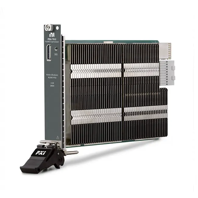
The PXIe-7912 is a PXI FlexRIO coprocessor module designed to add programmable, real-time signal processing to PXI Express systems. It combines a Xilinx Kintex UltraScale KU040 FPGA, 4 GB of onboard DRAM and a PCI Express Gen 3 x8 interface.
Using peer-to-peer streaming, the PXIe-7912 can transfer data between compatible PXI Express instruments at rates up to 7 GB/s without routing all data through the host controller. It is suitable for RF processing, spectral analysis, radar prototyping, data reduction, custom triggering and computationally demanding automated test systems.
Key Features of the PXIe-7912
- Xilinx Kintex UltraScale KU040 FPGA
- 242,200 FPGA lookup tables
- 1,920 DSP48 slices
- 21.1 Mb of embedded block RAM
- 4 GB onboard DRAM
- Maximum theoretical DRAM bandwidth of 17 GB/s
- PCI Express Gen 3 x8 interface
- Peer-to-peer streaming at up to 7 GB/s
- Eight bidirectional single-ended digital I/O channels
- Four high-speed serial transmit channels
- Four high-speed serial receive channels
- Serial data rates from 500 Mb/s to 16.375 Gb/s
- 60 DMA channels
- Support for PXI timing and trigger resources
- Programmable using LabVIEW FPGA
- Support for development with Xilinx Vivado
PXIe-7912 Technical Specifications
| Product Model | PXIe-7912 |
|---|---|
| Part Number | 785173-01 |
| Product Type | PXI FlexRIO Coprocessor Module |
| FPGA | Xilinx Kintex UltraScale KU040 |
| FPGA Slices | 60,600 |
| Lookup Tables | 242,200 |
| DSP48 Slices | 1,920 |
| Embedded Block RAM | 21.1 Mb |
| Onboard DRAM | 4 GB, arranged as two 2 GB banks |
| DRAM Clock Rate | 1,064 MHz |
| LabVIEW FPGA DRAM Clock | 267 MHz |
| Maximum Theoretical DRAM Rate | 17 GB/s total; 8.5 GB/s per bank |
| Bus Interface | PCI Express Gen 3 x8 |
| Maximum Peer-to-Peer Rate | Up to 7 GB/s |
| DMA Channels | 60 |
| Digital I/O Channels | 8 bidirectional single-ended channels |
| Digital Voltage Families | 1.2 V, 1.5 V, 1.8 V, 2.5 V and 3.3 V |
| Digital Output Toggle Rate | 60 MHz nominal with a 100 μA load |
| High-Speed Serial Channels | 4 transmit and 4 receive |
| High-Speed Serial Rate | 500 Mb/s to 16.375 Gb/s nominal |
| Front Connector | Molex Nano-Pitch I/O |
| Default FPGA Timebase | 80 MHz |
| Timebase Reference | PXI Express 100 MHz clock |
| Maximum Power Requirement | 58 W |
| Operating Temperature | 0°C to 55°C with adequate chassis slot cooling |
| Dimensions | 18.8 cm × 12.9 cm, excluding connectors |
| Weight | 190 g |
PXIe-7912 Part Number and Configuration
| Part Number | FPGA | DRAM | PXI Interface | Auxiliary I/O |
|---|---|---|---|---|
| 785173-01 | Kintex UltraScale KU040 | 4 GB | PCI Express Gen 3 x8 | 8 GPIO and 4 TX/4 RX high-speed serial lanes |
The PXIe-7912 has one primary hardware configuration. Verify part number 785173-01 when requesting pricing, technical support or a replacement module.
Kintex UltraScale KU040 FPGA
The PXIe-7912 uses a Xilinx Kintex UltraScale KU040 FPGA with 242,200 lookup tables, 1,920 DSP48 slices and 21.1 Mb of embedded block RAM.
The FPGA is suitable for a moderate amount of parallel signal processing and can implement customized algorithms directly in hardware.
- Digital filtering
- Fast Fourier transform processing
- Digital downconversion
- Frequency channelization
- Signal averaging
- Pulse and event detection
- Custom triggering
- Real-time data reduction
- Protocol processing
- Deterministic decision making
Some FPGA resources are reserved for PCI Express connectivity, device configuration and board-level interfaces, so the resources available to the user are slightly lower than the total device capacity.
4 GB Onboard DRAM
The PXIe-7912 includes 4 GB of onboard DRAM arranged as two independent 2 GB banks. Each bank provides a maximum theoretical data rate of 8.5 GB/s, producing a combined theoretical rate of 17 GB/s.
Onboard memory can be used for:
- High-speed waveform buffering
- Temporary acquisition storage
- Record-based signal processing
- Long digital delay lines
- Channel emulation
- Large lookup tables
- Multistage FPGA algorithms
The LabVIEW FPGA memory interface simplifies access to DRAM without requiring the user to manage every low-level memory transaction.
7 GB/s Peer-to-Peer Streaming
The PCI Express Gen 3 x8 architecture allows the PXIe-7912 to stream data to and from compatible PXI Express modules at rates up to 7 GB/s.
Peer-to-peer streaming transfers data directly between modules without sending it through the host controller. This reduces CPU workload and helps maintain low-latency data paths for high-throughput applications.
The PXIe-7912 can be paired with oscilloscopes, digitizers, RF instruments, vector signal transceivers and other FPGA-enabled PXI modules.
FPGA Coprocessing for PXI Instruments
The PXIe-7912 does not contain a dedicated analog measurement front end. Instead, it acts as an FPGA coprocessor for data acquired or generated by other PXI instruments.
A compatible source instrument can stream data to the PXIe-7912, where the FPGA processes the data before transferring results to another module, system memory or storage device.
This architecture is useful when an existing instrument does not provide sufficient onboard FPGA resources for the required algorithm.
Eight Bidirectional Digital I/O Channels
The front-panel Nano-Pitch connector provides eight bidirectional single-ended digital I/O channels. Each channel supports independent direction control.
Supported voltage families include 1.2 V, 1.5 V, 1.8 V, 2.5 V and 3.3 V. The maximum nominal output toggle rate is 60 MHz with a 100 μA load.
These lines can be used for external triggering, status signals, control interfaces and communication with custom electronics.
High-Speed Serial I/O
The PXIe-7912 provides four high-speed serial transmit channels and four receive channels through its front-panel connector.
The Xilinx UltraScale GTH transceivers support nominal data rates from 500 Mb/s to 16.375 Gb/s. They can be used for custom serial interfaces, FPGA-to-FPGA communication and high-bandwidth data transfer to external hardware.
PXI Timing and Trigger Resources
The PXIe-7912 can access multiple timing and trigger resources through the PXI Express backplane:
- PXI trigger lines
- PXI_CLK10
- PXI star trigger
- PXIe_DStarB
- PXIe_DStarC
- PXIe_Sync100
These resources help coordinate FPGA processing with other acquisition, generation and RF modules in a synchronized PXI system.
60 DMA Channels
The PXIe-7912 provides 60 DMA channels for transferring data between FPGA logic and other system components. Multiple DMA channels allow FPGA applications to maintain several independent data streams.
Appropriate DMA configuration can separate raw data, processed results, status information and control messages into independent transfer paths.
Typical PXIe-7912 Applications
- Real-time RF signal processing
- Vector signal transceiver coprocessing
- Digital downconversion
- Wideband spectral analysis
- Radar and electronic warfare prototyping
- Channelization and signal classification
- High-speed event detection
- Data reduction before storage
- FPGA-to-FPGA streaming
- Custom protocol processing
- Hardware-in-the-loop testing
- Semiconductor validation
- High-throughput automated test systems
Software Support
The PXIe-7912 is supported by NI LabVIEW Instrument Design Libraries for FlexRIO. These libraries provide interfaces, documentation and sample projects for configuring the device and developing real-time FPGA applications.
- LabVIEW
- LabVIEW FPGA Module
- Instrument Design Libraries for FlexRIO
- NI FlexRIO driver
- Xilinx Vivado development tools
Engineers can develop FPGA logic through LabVIEW FPGA or use supported Xilinx development workflows when integrating existing HDL code and specialized FPGA intellectual property.
PXI Express Chassis Requirements
The PXIe-7912 requires a compatible PXI Express chassis and a Gen 3 x8-capable peripheral slot to achieve maximum data-transfer performance.
The chassis slot must provide at least 58 W of cooling capacity. Not every chassis supporting 58 W slot cooling can maintain the full 0°C to 55°C module operating range, so verify the chassis specifications.
Browse compatible NI PXI modules and system components when configuring a complete FPGA processing platform.
PXIe-7912 Troubleshooting
Why is the peer-to-peer transfer rate lower than 7 GB/s?
Confirm that both modules support peer-to-peer streaming and are installed in chassis slots with a compatible Gen 3 x8 data path. Chassis topology, FPGA logic and transfer-block size can affect throughput.
Why is the high-speed serial interface unavailable?
Verify that the FPGA personality enables the required GTH transceivers and that the cable, connector and external device support the configured line rate.
Why is the FPGA compilation unsuccessful?
Confirm that the design fits within the KU040 lookup tables, DSP slices and block RAM. Reduce parallel processing or memory requirements if the design exceeds the available resources.
Why does the module revert to its default FPGA personality?
A large FPGA design operating at high clock rates can exceed the module’s available power. Verify the chassis cooling capacity and optimize the FPGA implementation.
Why is the module not visible in software?
Confirm that it is installed in a compatible PXI Express slot. Check the chassis, controller, FlexRIO driver, operating system and software version compatibility.
Why is DRAM performance lower than expected?
DRAM performance depends on access patterns, transfer size, arbitration and FPGA logic. Sequential, burst-based transfers generally provide better throughput than frequent small or random transactions.
Can the PXIe-7912 acquire analog signals directly?
No. The PXIe-7912 is a coprocessor module without an integrated analog front end. It processes data received from other PXI instruments or external digital interfaces.
PXIe-7912 Comparison
| Model | FPGA | DRAM | PXI Interface | Auxiliary I/O | Primary Difference |
|---|---|---|---|---|---|
| PXIe-7912 | Kintex UltraScale KU040 | 4 GB | Gen 3 x8 | 8 GPIO and 4 TX/4 RX HSS | Moderate FPGA processing capacity with DRAM and serial I/O |
| PXIe-7911 | Kintex UltraScale KU035 | None | Gen 3 x8 | No front-panel auxiliary I/O | Smaller FPGA configuration without external DRAM |
| PXIe-7915 | Kintex UltraScale KU060 | 4 GB | Gen 3 x8 | 8 GPIO and 4 TX/4 RX HSS | Larger FPGA for more demanding parallel processing |
| PXIe-7976 | Kintex-7 410T | 2 GB | Gen 2 x8 | FlexRIO adapter interface | Designed for use with modular FlexRIO adapter modules |
| PXIe-7902 | Virtex-7 485T | 2 GB | Gen 2 x8 | 24 TX/RX serial lanes | Dedicated high-speed serial protocol testing |
Recommended Related Products
- PXIe-7911 – Suitable for applications requiring a smaller KU035 FPGA without onboard DRAM or auxiliary I/O.
- PXIe-7915 – Recommended when the larger KU060 FPGA is required for more complex RF and signal-processing algorithms.
- PXIe-7976 – Provides a modular FlexRIO FPGA platform for use with compatible analog and digital adapter modules.
- PXIe-7902 – Designed for applications requiring 24 high-speed serial transmit and receive lanes.
How to Select the Right PXI FPGA Coprocessor
- Choose the PXIe-7912 for moderate FPGA processing with 4 GB DRAM and front-panel GPIO and serial I/O.
- Choose the PXIe-7911 when onboard DRAM and auxiliary I/O are unnecessary.
- Choose the PXIe-7915 for larger algorithms requiring additional LUTs, DSP slices and block RAM.
- Choose a PXIe-797x module when the application requires a modular FlexRIO analog or digital adapter.
- Choose a high-speed serial instrument when multiple dedicated serial protocol lanes are required.
Why Choose the PXIe-7912?
The PXIe-7912 combines a programmable KU040 FPGA, 4 GB DRAM, Gen 3 x8 PXI connectivity and high-speed serial I/O in a compact coprocessor module. It adds deterministic processing capacity without requiring replacement of the source measurement instrument.
Its peer-to-peer architecture is particularly valuable in systems where large data streams must be processed in real time before transfer to the host controller or storage device.
Frequently Asked Questions
What is the PXIe-7912?
The PXIe-7912 is a Kintex UltraScale KU040 FPGA coprocessor module that adds real-time signal processing and high-speed data movement to PXI Express systems.
What is the PXIe-7912 part number?
The standard NI part number is 785173-01.
How much onboard memory does it provide?
The PXIe-7912 includes 4 GB of DRAM arranged as two 2 GB banks.
What is the maximum peer-to-peer streaming rate?
The module can stream data to and from compatible PXI Express devices at rates up to 7 GB/s.
Does the PXIe-7912 have analog inputs?
No. It is an FPGA coprocessor rather than a measurement instrument. Analog data must be supplied by another compatible PXI module.
What FPGA does the PXIe-7912 use?
It uses a Xilinx Kintex UltraScale KU040 FPGA with 242,200 LUTs, 1,920 DSP48 slices and 21.1 Mb of block RAM.
Does it provide digital I/O?
Yes. It provides eight bidirectional GPIO channels plus four high-speed serial transmit and four receive channels.
Can the PXIe-7912 be programmed with Vivado?
Yes. Depending on the development workflow, it can be programmed using LabVIEW FPGA or supported Xilinx Vivado tools.
What is the difference between the PXIe-7912 and PXIe-7915?
Both provide 4 GB DRAM, Gen 3 x8 connectivity and similar auxiliary I/O. The PXIe-7915 uses a larger KU060 FPGA for more demanding processing.
Can the PXIe-7912 operate independently?
No. It requires a compatible PXI Express chassis, controller or peer-to-peer source module and the appropriate software environment.
Request a Quote for the PXIe-7912
Contact us for current availability, lead time and project pricing for the PXIe-7912 PXI FlexRIO Coprocessor Module. We can also help verify compatible PXI chassis, controllers, RF instruments and peer-to-peer streaming configurations.















