







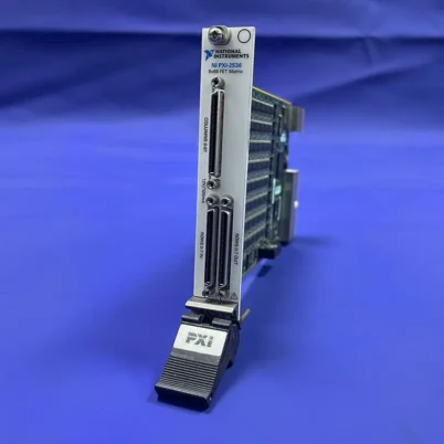
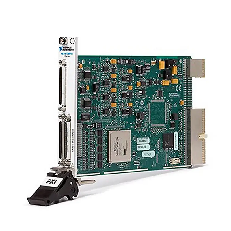
PXI-7851 Multifunction Reconfigurable I/O Module
The PXI-7851, also known as the PXI-7851R, is a multifunction reconfigurable I/O module featuring a user-programmable Xilinx Virtex-5 LX30 FPGA. It combines analog input, analog output and digital I/O resources with direct FPGA control for deterministic measurement and control applications.
The module provides eight 16-bit analog inputs with independent sampling rates up to 750 kS/s per channel, eight 16-bit analog outputs at up to 1 MS/s per channel and 96 bidirectional digital I/O lines.
Key Features of the PXI-7851
- Xilinx Virtex-5 LX30 user-programmable FPGA
- Eight 16-bit analog input channels
- 750 kS/s maximum sampling rate per analog input
- Dedicated ADC for every analog input channel
- Eight 16-bit analog output channels
- 1 MS/s maximum update rate per analog output
- ±10 V analog input and output ranges
- 96 bidirectional TTL digital I/O lines
- Programmable digital power-on states
- Independent channel timing and triggering
- Support for multirate analog acquisition
- Three 68-pin VHDCI I/O connectors
- PXI Hybrid bus interface
- Programmable with the LabVIEW FPGA Module
PXI-7851 Technical Specifications
| Product Model | PXI-7851 / PXI-7851R |
|---|---|
| Part Number | 780339-01 |
| Product Type | Multifunction Reconfigurable I/O Module |
| Product Family | NI R Series Multifunction RIO |
| Bus Interface | PXI Hybrid |
| FPGA | Xilinx Virtex-5 LX30 |
| FPGA Flip-Flops | 19,200 |
| FPGA 6-Input LUTs | 19,200 |
| DSP48 Slices | 32 |
| Embedded Block RAM | 1,152 kbits |
| Analog Input Channels | 8 |
| Analog Input Resolution | 16 bits |
| Maximum Analog Input Rate | 750 kS/s per channel |
| Analog Input Range | ±10 V |
| Input Modes | Differential, RSE or NRSE |
| Analog Output Channels | 8 |
| Analog Output Resolution | 16 bits |
| Maximum Analog Output Rate | 1 MS/s per channel |
| Analog Output Range | ±10 V |
| Digital I/O Channels | 96 bidirectional lines |
| Digital Compatibility | TTL, 3.3 V output and 5 V input compatible |
| Digital Output Current | 4 mA source or sink |
| Maximum Clock Rate | 40 MHz base clock |
| Onboard DRAM | None |
| I/O Connectors | 3 × 68-pin female VHDCI |
| Operating Temperature | 0°C to 55°C |
| Dimensions | 16 × 10 cm, standard 3U PXI module |
| Weight | Approximately 152 g |
| Product Status | Mature; not recommended for new designs |
PXI-7851 Part Number and Configuration
| Model | Part Number | Configuration |
|---|---|---|
| PXI-7851 | 780339-01 | Virtex-5 LX30 FPGA, 8 AI, 8 AO and 96 digital I/O |
User-Programmable Virtex-5 FPGA
The PXI-7851 uses a Xilinx Virtex-5 LX30 FPGA that can be programmed with the LabVIEW FPGA Module. Custom FPGA logic can directly control I/O timing, triggering, signal processing and communication protocols without relying on nondeterministic host-computer timing.
The FPGA includes 19,200 flip-flops, 19,200 six-input lookup tables, 32 DSP48 slices and 1,152 kbits of embedded block RAM. These resources support custom control loops, digital filtering, mathematical processing and protocol logic.
Eight Independent Analog Inputs
The PXI-7851 provides eight 16-bit analog input channels with a ±10 V range. Each channel has a dedicated successive-approximation ADC capable of sampling at up to 750 kS/s.
Because the channels do not share a multiplexed ADC, each input can use independent timing and triggering. This design supports simultaneous acquisition, individual channel triggers and multirate sampling that conventional multifunction DAQ devices may not provide.
Analog Input Connection Modes
The analog input channels support differential, referenced single-ended and nonreferenced single-ended connection modes. The selected input mode applies to all analog input channels.
- Differential: Provides improved noise rejection for floating or low-level signals.
- RSE: References input signals to the device analog ground.
- NRSE: References input signals to a shared remote-sense connection.
The appropriate wiring configuration depends on signal grounding, source impedance, cable length and the electrical noise present in the test system.
Eight Analog Outputs
The PXI-7851 provides eight single-ended, 16-bit voltage outputs with a ±10 V range. Each channel supports update rates up to 1 MS/s and can be controlled directly from the FPGA.
These outputs can generate control signals, simulate sensors, provide actuator commands and produce custom waveforms. The power-on output state can be configured according to the safety requirements of the application.
96 Bidirectional Digital I/O Lines
The module includes 96 TTL-compatible digital I/O lines. Direction and power-on state can be configured by line, allowing the digital resources to implement custom interfaces, timing signals, triggers and control functions.
Digital outputs operate at 3.3 V logic levels, while inputs can accept compatible signals up to 5.5 V. Each line can source or sink up to 4 mA within the device specifications.
Deterministic Timing and Control
FPGA-based execution provides hardware-timed response without interruption from a desktop operating system. Control algorithms, safety interlocks and custom triggers can execute directly on the module with predictable timing.
The PXI-7851 is especially useful when standard DAQ timing engines cannot provide the required channel independence, control-loop speed or custom digital behavior.
Typical PXI-7851 Applications
- Hardware-in-the-loop simulation
- High-speed closed-loop control
- Custom digital protocol implementation
- Sensor and actuator simulation
- Automotive electronic control unit testing
- Aerospace system validation
- Power electronics testing
- Machine condition monitoring
- Custom data acquisition systems
- Research and rapid control prototyping
- Electronic device functional testing
LabVIEW FPGA Programming
The PXI-7851 is programmed using the LabVIEW FPGA Module and a compatible R Series driver. Engineers can create custom hardware personalities for analog acquisition, waveform generation, digital communication and deterministic control.
A host application can communicate with the compiled FPGA personality to configure tests, transfer data and display results. Because FPGA compilation can require substantial time, the I/O architecture and resource allocation should be planned before beginning a large application.
Multirate Sampling and Individual Triggering
Dedicated ADCs allow different analog input channels to operate at different effective rates. Engineers can acquire faster-changing signals at higher rates while sampling slower sensor signals less frequently.
Trigger logic can also be implemented independently for individual channels. This provides more flexibility than conventional multiplexed DAQ devices that share one conversion clock and trigger configuration across several inputs.
VHDCI Connectivity and Accessories
The PXI-7851 provides three 68-pin female high-density VHDCI connectors. Compatible shielded cables and connector blocks are required to access the analog and digital signals.
NI SCB-68 or SCB-68A connector blocks may be used with the correct R Series pinout labels and compatible cables. The pinout differs from conventional DAQ devices, so the PXI-7851 wiring diagram must be verified before connecting signals.
The NI-9151 R Series expansion chassis can connect to compatible digital connectors and add signal-conditioned C Series I/O modules. One PXI-7851 can support up to two compatible NI-9151 expansion chassis.
PXI Chassis Integration
The PXI-7851 installs in a compatible PXI or PXI Hybrid chassis. It can be synchronized with other PXI instruments through chassis timing and triggering resources.
The module does not include onboard DRAM. Applications requiring high-volume data buffering should consider FPGA block RAM limits, DMA transfers and host-controller performance during system design.
PXI-7851 Troubleshooting
The module is not detected in NI MAX
Confirm that the PXI-7851 is fully seated in a compatible PXI or PXI Hybrid slot. Verify the chassis, controller, R Series driver and LabVIEW FPGA support, then refresh the device list in NI Measurement & Automation Explorer.
The FPGA VI will not compile
Check that the installed LabVIEW FPGA version supports the PXI-7851 and its Virtex-5 compilation tools. Review FPGA resource usage if the design exceeds the available LUT, register, DSP or block RAM capacity.
Analog input readings are noisy
Select the appropriate differential or single-ended input mode, use shielded cables and review grounding. Keep analog wiring away from switching power supplies, motors and high-current digital lines.
Analog input channels do not sample at the expected rate
Verify that each FPGA I/O node and loop are configured for the intended timing. Account for FPGA processing, DMA transfer and host-reading requirements when calculating sustained acquisition rates.
Digital signals are not recognized correctly
Confirm the external logic voltage, grounding and input thresholds. The outputs use 3.3 V logic, while the inputs are compatible with supported 3.3 V and 5 V TTL signals.
The connector-block signals do not match the FPGA channels
Use the PXI-7851-specific VHDCI connector pinout. Do not assume that a standard DAQ device or another R Series model uses the same connector-block channel mapping.
PXI-7851 Compared with Related R Series Modules
| Model | FPGA | Analog Input Rate | I/O Configuration | Best Suited For |
|---|---|---|---|---|
| PXI-7851 | Virtex-5 LX30 | 750 kS/s | 8 AI, 8 AO, 96 DIO | FPGA-based multifunction control |
| PXI-7841 | Virtex-5 LX30 | 200 kS/s | 8 AI, 8 AO, 96 DIO | Lower-speed multifunction FPGA applications |
| PXI-7852 | Virtex-5 LX50 | 750 kS/s | 8 AI, 8 AO, 96 DIO | Applications requiring more FPGA resources |
| PXI-7853 | Virtex-5 LX85 | 750 kS/s | 8 AI, 8 AO, 96 DIO | Larger FPGA processing designs |
| PXI-7854 | Virtex-5 LX110 | 750 kS/s | 8 AI, 8 AO, 96 DIO | Maximum FPGA capacity in the legacy family |
| PXIe-7847 | Kintex-7 | Higher-performance generation | Multifunction analog and digital I/O | Newer PXI Express FPGA systems |
Recommended Related Products
- PXI-7841 Multifunction RIO Module – A lower-speed Virtex-5 LX30 alternative with a similar I/O configuration.
- PXI-7852 Multifunction RIO Module – A 750 kS/s module with a larger Virtex-5 LX50 FPGA.
- PXI-7853 Multifunction RIO Module – A Virtex-5 LX85 model for applications requiring additional FPGA resources.
- PXI-7854 Multifunction RIO Module – A Virtex-5 LX110 version for larger FPGA designs.
- PXIe-7847 Multifunction Reconfigurable I/O Module – A newer Kintex-7-based PXI Express alternative.
- PXIe-1092 PXI Express Chassis – A modular chassis for synchronized measurement and control systems.
Additional FPGA, data acquisition and control products are available in the NI PXI Modules category.
Selecting the PXI-7851
Choose the PXI-7851 when maintaining or expanding a system that requires eight 750 kS/s analog inputs, eight high-speed analog outputs, 96 digital lines and direct Virtex-5 FPGA control.
The PXI-7851 has mature product status and is not recommended for new system designs. For a new application, compare current Kintex-7 R Series PXI Express modules according to required analog performance, digital I/O voltage and FPGA capacity.
Why Choose the PXI-7851?
- Combines analog input, analog output and digital I/O
- Provides a dedicated ADC for every analog input
- Supports deterministic FPGA-based processing
- Allows custom timing, triggering and protocols
- Supports multirate sampling and independent channel triggers
- Provides 96 configurable digital I/O lines
- Integrates with existing PXI R Series systems
Frequently Asked Questions
What is the PXI-7851 used for?
The PXI-7851 is used for FPGA-based data acquisition, hardware-in-the-loop testing, custom digital protocols, sensor simulation and deterministic control.
How many analog channels does the PXI-7851 provide?
It provides eight 16-bit analog inputs and eight 16-bit analog outputs.
What is the maximum analog input sampling rate?
Each analog input channel can sample at rates up to 750 kS/s using its dedicated ADC.
What is the analog output update rate?
Each analog output supports update rates up to 1 MS/s with 16-bit resolution.
How many digital I/O lines are available?
The PXI-7851 provides 96 bidirectional TTL-compatible digital I/O lines.
Which FPGA does the PXI-7851 use?
The module uses a Xilinx Virtex-5 LX30 FPGA with 19,200 flip-flops, 32 DSP48 slices and 1,152 kbits of embedded block RAM.
Does the PXI-7851 have onboard DRAM?
No. The PXI-7851 does not include onboard DRAM. It uses FPGA block RAM and DMA communication with the host system.
What software is required?
FPGA customization requires a compatible version of LabVIEW FPGA and the supported NI R Series driver. A host application is typically created in LabVIEW or another supported environment.
What is the part number for the PXI-7851?
The standard NI part number for the PXI-7851 is 780339-01.
Request a Quote for the PXI-7851
Contact us for current availability, condition, lead time and project pricing for the PXI-7851 Multifunction Reconfigurable I/O Module. We can also help identify compatible VHDCI cables, connector blocks, PXI chassis and newer R Series replacement options.















