






Product Introduction
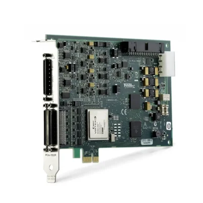
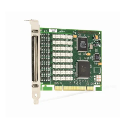
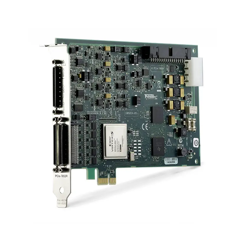
The NI PCIe-7842R, commonly referenced as PCIe-7842, is an R Series Multifunction Reconfigurable I/O (RIO) device designed for hardware-in-the-loop (HIL) testing, automated test, custom digital protocols, sensor simulation, high-speed control, and FPGA-based measurement applications.
The PCIe-7842R combines analog input, analog output, digital I/O, and a user-programmable Xilinx Virtex-5 LX50 FPGA on a PCI Express platform. The onboard FPGA allows engineers to implement custom timing, triggering, signal processing, digital communication, and control algorithms directly in hardware.
With 8 analog inputs, 8 analog outputs, up to 200 kS/s analog input sampling, and 96 bidirectional digital I/O lines, the PCIe-7842R provides a flexible FPGA-based interface for complex mixed-signal test and control systems.
Product Overview
The National Instruments PCIe-7842R belongs to the NI R Series Multifunction RIO family.
A typical system architecture is:
Sensors / DUT → PCIe-7842R I/O → Virtex-5 FPGA → PCI Express → Host Computer
Unlike conventional multifunction DAQ devices, time-critical measurement and control functions can execute directly on the FPGA without depending on the timing behavior of the host operating system.
This architecture makes the PCIe-7842R suitable for deterministic measurement, hardware-in-the-loop simulation, custom interfaces, and high-speed control applications.
Key Features
Xilinx Virtex-5 LX50 FPGA
The PCIe-7842R incorporates a user-programmable Xilinx Virtex-5 LX50 FPGA.
The FPGA can implement application-specific functions such as:
- Custom hardware triggering
- Deterministic control loops
- Digital signal processing
- Custom digital protocols
- Sensor simulation
- Event detection
- Custom timing engines
- Hardware interlocks
- Parallel processing
- Data reduction
8 Analog Input Channels
The PCIe-7842R provides 8 analog input channels for acquiring voltage signals from sensors, devices under test, and external signal-conditioning hardware.
Typical analog input applications include:
- Sensor acquisition
- Electronic validation
- HIL testing
- Control feedback
- Automated test
- Experimental measurement
Dedicated ADC per Analog Input Channel
Each analog input channel uses a dedicated analog-to-digital converter rather than sharing a single ADC through a conventional multiplexer.
This architecture enables:
- Simultaneous multi-channel acquisition
- Independent channel timing
- Custom FPGA-controlled sampling
- Deterministic acquisition
- Parallel signal processing
200 kS/s Analog Input Sampling
The PCIe-7842R supports analog input sampling rates up to 200 kS/s per channel.
Combined with dedicated ADCs, this allows multiple analog signals to be acquired simultaneously while preserving their timing relationships.
16-Bit Analog Input Resolution
The analog input subsystem provides 16-bit resolution for general measurement and control applications.
This combination of resolution, simultaneous sampling, and FPGA-based processing makes the PCIe-7842R useful for applications where deterministic multi-channel measurement is more important than extremely high digitizer sampling rates.
8 Analog Output Channels
The PCIe-7842R provides 8 analog output channels for generating programmable voltage signals.
Analog outputs can be used for:
- Sensor simulation
- Device stimulus
- Closed-loop control
- HIL simulation
- Analog waveform generation
- Automated test
16-Bit Analog Output Resolution
The analog output channels provide 16-bit resolution, enabling programmable voltage generation for compatible test, simulation, and control applications.
96 Bidirectional Digital I/O Lines
The PCIe-7842R provides 96 bidirectional digital I/O lines.
These digital channels can be controlled directly by FPGA logic for deterministic digital operations.
Applications include:
- DUT control
- Status monitoring
- Digital stimulus generation
- Custom protocol implementation
- Hardware triggering
- Pulse generation
- Digital sensor simulation
- Test fixture control
40 MHz Digital I/O
The digital I/O subsystem supports FPGA-controlled operation at rates up to approximately 40 MHz, depending on the application, signal configuration, and FPGA implementation.
This enables the PCIe-7842R to implement custom high-speed digital interfaces that are difficult to reproduce using software-timed digital I/O.
PCI Express Interface
The PCIe-7842R installs in a compatible PCI Express slot.
PCI Express provides communication between the FPGA-based measurement hardware and the host computer for configuration, data transfer, monitoring, and higher-level application processing.
Deterministic FPGA Processing
Critical measurement and control functions can execute directly on the FPGA.
A simplified architecture is:
Input Signal → FPGA Processing → Decision Logic → Output Response
This architecture provides predictable hardware-level response without requiring every operation to pass through the host operating system.
Technical Specifications
| Parameter | Specification |
|---|---|
| Product Type | R Series Multifunction Reconfigurable I/O Device |
| Model | PCIe-7842 / PCIe-7842R |
| Manufacturer | National Instruments |
| Bus Interface | PCI Express |
| FPGA | Xilinx Virtex-5 LX50 |
| Analog Input Channels | 8 |
| Analog Input Resolution | 16 Bit |
| Maximum Analog Input Sample Rate | 200 kS/s per Channel |
| Analog Input Architecture | Dedicated ADC per Channel / Simultaneous Sampling |
| Analog Output Channels | 8 |
| Analog Output Resolution | 16 Bit |
| Digital I/O | 96 Bidirectional Lines |
| Maximum Digital I/O Rate | Up to 40 MHz |
| FPGA Programmable | Yes |
| Custom Triggering | Supported Through FPGA |
| Parallel Processing | Supported |
| Primary Programming Environment | LabVIEW FPGA |
| Primary Applications | HIL Testing, Sensor Simulation, Custom Protocols, Automated Test and High-Speed Control |
How Does the PCIe-7842R Work?
The PCIe-7842R combines physical analog and digital I/O with a programmable FPGA.
A simplified measurement path is:
Physical Signal → PCIe-7842R I/O → Virtex-5 FPGA → Custom Processing → PCI Express → Host Application
For deterministic control:
Sensor Input → FPGA → Control Algorithm → Analog / Digital Output → DUT
This allows measurement, processing, and output response to occur directly in hardware.
What Is an R Series Multifunction RIO Device?
An R Series Multifunction RIO device combines analog and digital I/O with a user-programmable FPGA.
Compared with conventional multifunction DAQ hardware, R Series devices allow engineers to customize hardware behavior rather than relying only on predefined acquisition and generation functions.
FPGA customization can include:
- Custom sampling architectures
- Custom trigger conditions
- Signal processing
- Digital communication protocols
- Deterministic control
- Hardware state machines
- Safety and interlock logic
Simultaneous Analog Input Sampling
The PCIe-7842R uses dedicated ADC resources for its analog input channels.
A simplified architecture is:
AI0 → ADC0
AI1 → ADC1
AI2 → ADC2
AI3 → ADC3
… → Dedicated ADCs
This differs from multiplexed DAQ devices where several channels share one ADC.
Dedicated ADCs make the PCIe-7842R suitable for measurements where channel-to-channel timing relationships must be preserved.
FPGA-Based Real-Time Processing
The Virtex-5 FPGA can process measurement data before transferring it to the host computer.
Possible FPGA processing functions include:
- Digital filtering
- Threshold detection
- Event detection
- Scaling
- Control algorithms
- Custom trigger evaluation
- Signal comparison
- Data reduction
This can reduce host processing requirements and provide deterministic response.
Parallel FPGA Processing
Unlike sequential software execution, FPGA logic can execute many operations in parallel.
For example, the PCIe-7842R can simultaneously:
- Acquire analog channels
- Generate analog outputs
- Monitor digital inputs
- Control digital outputs
- Evaluate trigger conditions
- Execute control algorithms
- Transfer selected data to the host
Hardware-in-the-Loop Testing
The PCIe-7842R can be used as an FPGA-based I/O interface in hardware-in-the-loop testing.
A typical HIL architecture is:
Simulation Model → PCIe-7842R FPGA → Simulated Sensor / Actuator I/O → Controller / DUT
Typical HIL applications include:
- ECU validation
- Embedded controller testing
- Industrial control testing
- Power electronics testing
- Controller fault testing
- Prototype validation
Sensor Simulation
The combination of analog outputs, digital I/O, and programmable FPGA logic makes the PCIe-7842R suitable for sensor simulation.
Possible simulated signals include:
- Analog voltage sensors
- Position sensors
- Speed sensors
- Pulse-output sensors
- Encoder-type signals
- Digital sensors
External conditioning circuitry may be required when the electrical characteristics of the simulated sensor differ from the native PCIe-7842R I/O characteristics.
High-Speed Control
The PCIe-7842R can execute closed-loop control algorithms directly on its FPGA.
A typical architecture is:
Sensor → Analog Input → FPGA Control Algorithm → Analog / Digital Output → Plant
FPGA implementation can provide deterministic loop timing for applications that cannot tolerate operating-system scheduling delays.
Custom Protocol Communication
The 96 FPGA-controlled digital I/O lines can be used to implement custom or proprietary digital communication interfaces.
Applications can include:
- Custom serial protocols
- Parallel digital interfaces
- Legacy equipment communication
- Proprietary device protocols
- Custom command sequences
- FPGA-based protocol emulation
Custom Triggering
The programmable FPGA allows engineers to develop application-specific trigger conditions.
Triggers can be based on:
- Analog thresholds
- Digital input states
- Multiple simultaneous conditions
- Timing relationships
- Sequential events
- Calculated FPGA conditions
Analog Output Applications
The eight analog outputs provide substantial flexibility for test and simulation applications.
A typical stimulus-response architecture is:
PCIe-7842R AO → DUT → PCIe-7842R AI → FPGA Processing
This allows one device to generate stimulus signals, measure responses, and execute custom FPGA processing.
Digital I/O Applications
The 96 bidirectional digital lines provide high channel density for FPGA-based digital control.
Typical applications include:
- DUT configuration
- Production fixture control
- Relay control
- Status monitoring
- Pulse generation
- Custom protocols
- Digital sensor simulation
- Hardware synchronization
Automated Test
The PCIe-7842R can integrate several functions into one automated test interface.
A typical test sequence can:
- Configure digital DUT controls.
- Generate analog stimulus signals.
- Acquire multiple analog responses simultaneously.
- Process measurements on the FPGA.
- Evaluate custom trigger conditions.
- Generate deterministic output responses.
- Transfer test data to the host computer.
- Determine pass or fail status.
PCIe-7842R vs Conventional Multifunction DAQ
| Feature | PCIe-7842R | Conventional DAQ |
|---|---|---|
| User-Programmable FPGA | Yes | Usually No |
| Analog Input Architecture | Dedicated ADCs | Often Multiplexed |
| Custom Hardware Timing | Yes | Fixed Functions |
| Custom Trigger Logic | FPGA Programmable | Predefined |
| Deterministic Processing | On FPGA | Primarily Host-Based |
| Custom Digital Protocols | Supported | Limited |
| Typical Application | HIL / Control / Custom I/O | General Data Acquisition |
PCIe-7842R vs PCIe-7841R
The PCIe-7842R and PCIe-7841R belong to the same generation of NI R Series multifunction reconfigurable I/O devices.
When selecting or replacing these devices, compare:
- FPGA resources
- Analog input requirements
- Analog output requirements
- Digital I/O requirements
- Existing FPGA bitfile
- Application timing requirements
- LabVIEW FPGA compatibility
For an existing automated test or HIL system, the FPGA target and compiled application should be verified before replacing one R Series model with another.
PCIe-7842R vs Newer Kintex-7 R Series
The PCIe-7842R uses an older Virtex-5 FPGA architecture, while newer R Series devices use more recent Kintex-7 FPGA technology.
| Feature | PCIe-7842R | Newer Kintex-7 R Series |
|---|---|---|
| FPGA Generation | Virtex-5 | Kintex-7 |
| Existing Legacy Code | Strong Fit for Existing Systems | May Require Migration |
| FPGA Resources | Legacy Generation | Generally Greater |
| New System Development | Legacy Applications | Usually Preferred |
| Replacement Considerations | Existing Bitfile / Wiring | Software and Hardware Migration |
PCIe-7842R Connectivity
The PCIe-7842R uses high-density connectors to provide access to its analog and digital I/O resources.
When integrating or replacing the device, verify:
- Connector pinout
- Existing SHC68-series cables
- Terminal blocks
- Analog signal wiring
- Digital I/O assignments
- Grounding configuration
- External signal conditioning
Cable and terminal-block compatibility should be checked against the exact PCIe-7842R hardware configuration before installation.
LabVIEW FPGA Integration
The PCIe-7842R is designed for use with compatible versions of the LabVIEW FPGA Module.
LabVIEW FPGA can be used to implement:
- Analog acquisition
- Analog generation
- Digital I/O control
- Custom timing
- Triggering
- Signal processing
- Closed-loop control
- Custom communication protocols
- Hardware state machines
Because the PCIe-7842R is a legacy FPGA platform, compatibility between the hardware, LabVIEW version, LabVIEW FPGA Module, FPGA compilation tools, drivers, and operating system should be verified carefully.
Legacy System Replacement
The PCIe-7842R is commonly found in legacy automated test, HIL, research, and industrial control systems.
When replacing an existing PCIe-7842R, verify:
- Exact model and part number
- Hardware revision
- Virtex-5 LX50 FPGA target
- Existing LabVIEW FPGA bitfile
- Analog input wiring
- Analog output wiring
- Digital I/O assignments
- Connector pinout
- Cable models
- Terminal blocks
- PCI Express slot compatibility
- LabVIEW version
- LabVIEW FPGA version
- FPGA compilation environment
- Driver support
- Operating system compatibility
A newer R Series device should not automatically be treated as a drop-in replacement because FPGA targets, connectors, timing behavior, drivers, and existing compiled FPGA applications may differ.
How to Choose an R Series Device
Before selecting the PCIe-7842R or a replacement R Series device, evaluate:
- Required analog input channels
- Required analog output channels
- Required sample rate
- Required analog resolution
- Digital I/O channel count
- FPGA resource requirements
- Deterministic control-loop requirements
- Custom protocol requirements
- Sensor simulation requirements
- HIL requirements
- Existing FPGA source code or bitfile
- PCI Express compatibility
- Cable and connector compatibility
- Software and driver support
Industries
- Automotive Testing
- Aerospace and Defense
- Industrial Automation
- Embedded Systems
- Power Electronics
- Automated Test
- Electronic Validation
- Research and Development
- Control-System Development
- Laboratory Automation
Applications
Hardware-in-the-Loop Testing
The PCIe-7842R provides deterministic FPGA-based analog and digital I/O for HIL systems used to validate controllers and embedded hardware.
Sensor Simulation
Eight analog outputs and FPGA-controlled digital I/O can be used to reproduce compatible sensor signals for DUT and controller validation.
High-Speed Control
Closed-loop control algorithms can execute directly on the FPGA for predictable and repeatable response timing.
Custom Protocol Communication
The 96 digital I/O lines can be controlled through custom FPGA logic for proprietary and application-specific communication interfaces.
Automated Test
Analog acquisition, analog generation, digital I/O, triggering, and FPGA processing can be combined within a single automated test interface.
Legacy Test System Maintenance
The PCIe-7842R can be important for maintaining existing systems where software, FPGA bitfiles, cabling, and test fixtures were originally developed around this specific R Series hardware platform.
Recommended Related Products
| PCIe-7842R | Virtex-5 LX50 FPGA-based R Series multifunction reconfigurable I/O device with 8 AI, 8 AO, and 96 DIO. |
| PCIe-7841R | Related Virtex-5 generation R Series multifunction RIO device for legacy FPGA measurement and control systems. |
| PCIe-7846 | Newer Kintex-7 generation R Series multifunction RIO device for FPGA-based HIL, control, and automated test applications. |
| PCIe-7855 | Kintex-7 R Series option for applications requiring newer FPGA architecture and higher analog acquisition performance. |
| PCIe-7856 | Higher-resource R Series device for demanding FPGA-based measurement, simulation, and control systems. |
Why Choose PCIe-7842R?
- Xilinx Virtex-5 LX50 FPGA
- User-programmable FPGA architecture
- 8 analog input channels
- Dedicated ADC per analog input channel
- Up to 200 kS/s per channel
- 16-bit analog input resolution
- 8 analog output channels
- 16-bit analog output resolution
- 96 bidirectional digital I/O lines
- Up to 40 MHz digital operation
- Simultaneous analog acquisition
- Custom hardware triggering
- Deterministic FPGA processing
- Parallel hardware processing
- Hardware-in-the-loop testing
- Sensor simulation
- Custom protocol implementation
- High-speed control
- PCI Express interface
- LabVIEW FPGA integration
Frequently Asked Questions
What is the NI PCIe-7842R?
The NI PCIe-7842R is an R Series PCI Express multifunction reconfigurable I/O device that combines analog input, analog output, digital I/O, and a user-programmable FPGA for deterministic measurement and control applications.
Is PCIe-7842 the same as PCIe-7842R?
The model is commonly referenced as both PCIe-7842 and PCIe-7842R. The “R” designation identifies the hardware as part of the NI R Series reconfigurable I/O family.
What FPGA does PCIe-7842R use?
The PCIe-7842R uses a Xilinx Virtex-5 LX50 FPGA.
How many analog inputs does PCIe-7842R have?
The PCIe-7842R provides 8 analog input channels.
What is the maximum analog input sample rate?
The PCIe-7842R supports analog input sampling rates up to 200 kS/s per channel.
Does PCIe-7842R support simultaneous sampling?
Yes. The analog input architecture uses dedicated ADC resources, allowing multiple analog input channels to be acquired simultaneously.
What is the analog input resolution?
The PCIe-7842R provides 16-bit analog input resolution.
How many analog outputs does PCIe-7842R have?
The device provides 8 analog output channels with 16-bit resolution.
How many digital I/O lines does PCIe-7842R have?
The PCIe-7842R provides 96 bidirectional digital I/O lines.
Can PCIe-7842R be used for HIL testing?
Yes. Its FPGA-based deterministic I/O architecture makes it suitable for hardware-in-the-loop testing and controller validation.
Can PCIe-7842R simulate sensors?
Yes. The analog outputs and FPGA-controlled digital I/O can be used for compatible sensor simulation applications. External signal conditioning may be required depending on the electrical characteristics of the simulated sensor.
Can PCIe-7842R implement custom digital protocols?
Yes. The programmable FPGA and digital I/O resources allow engineers to implement custom or proprietary digital communication protocols.
What software is used with PCIe-7842R?
The PCIe-7842R is designed for use with compatible NI R Series software and the LabVIEW FPGA Module.
Is PCIe-7842R a conventional DAQ card?
No. Although it provides analog and digital data acquisition, it is more accurately classified as an R Series Multifunction Reconfigurable I/O device because its FPGA allows users to customize hardware-level timing, processing, triggering, and control.
Is PCIe-7842R suitable for legacy system replacement?
Yes. The PCIe-7842R is particularly relevant for maintaining existing systems originally designed around this R Series platform. Matching the exact hardware can avoid substantial FPGA code, connector, wiring, driver, and test-fixture migration work.
Can a newer R Series card directly replace PCIe-7842R?
Not necessarily. A newer device may provide higher FPGA performance, but FPGA targets, I/O characteristics, connector pinouts, timing, software support, and existing compiled bitfiles may differ. Compatibility should be verified before migration.
What should I check before purchasing PCIe-7842R?
Verify the exact model and part number, Virtex-5 FPGA requirement, analog and digital I/O requirements, 200 kS/s sampling requirement, connector and cable configuration, existing LabVIEW FPGA source code or bitfile, PCI Express compatibility, NI driver version, LabVIEW FPGA version, FPGA compilation environment, and operating system compatibility.
Conclusion
The NI PCIe-7842R R Series Multifunction Reconfigurable I/O Device combines a Xilinx Virtex-5 LX50 FPGA, eight 16-bit analog inputs with dedicated ADCs and up to 200 kS/s per-channel sampling, eight 16-bit analog outputs, 96 bidirectional digital I/O lines, and PCI Express connectivity. Its programmable FPGA architecture makes it suitable for hardware-in-the-loop testing, sensor simulation, custom digital protocols, deterministic high-speed control, automated test, research, and legacy FPGA-based measurement systems.















