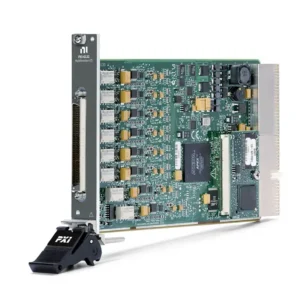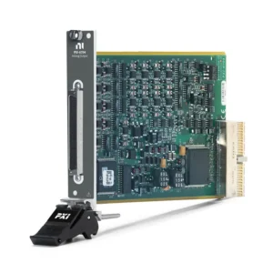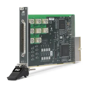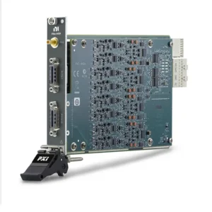


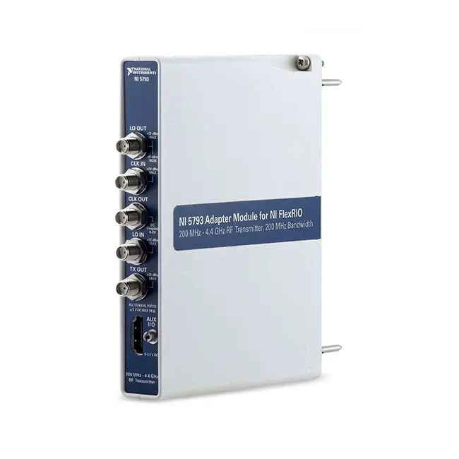
NI-5793 RF Transmitter Adapter Module for FlexRIO
The NI-5793 is a wideband RF transmitter adapter module designed for use with compatible NI FlexRIO FPGA hardware. It provides continuous RF output coverage from 200 MHz to 4.4 GHz with instantaneous bandwidth up to 200 MHz.
The direct-conversion transmitter uses dual 16-bit digital-to-analog converters for the I and Q baseband paths. An onboard synthesizer, programmable attenuation, selectable RF filters and external local-oscillator connections support customized waveform generation and synchronized multichannel RF systems.
Key Features of the NI-5793
- RF transmitter adapter module for FlexRIO
- 200 MHz to 4.4 GHz continuous frequency range
- 200 MHz instantaneous bandwidth at 6 dB
- 130 MHz instantaneous bandwidth at 3 dB
- Direct-conversion transmitter architecture
- Dual 16-bit I/Q DACs
- 250 MS/s native I/Q data rate
- 500 MS/s converter rate with 2× interpolation
- RF output up to +8 dBm nominal
- 0.25 dB nominal output-level resolution
- Integrated local-oscillator synthesizer
- LO input and output for synchronization
- Programmable FPGA signal processing
- Suitable for wideband RF research and prototyping
NI-5793 Technical Specifications
| Product Model | NI-5793 |
|---|---|
| Product Type | RF transmitter adapter module for FlexRIO |
| RF Frequency Range | 200 MHz to 4.4 GHz |
| Instantaneous Bandwidth | 200 MHz at 6 dB; 130 MHz at 3 dB |
| Transmitter Architecture | Single-stage direct conversion |
| DAC Configuration | Dual-channel I/Q DAC |
| DAC Resolution | 16 bits |
| Native I/Q Data Rate | Up to 250 MS/s |
| Interpolated DAC Rate | Up to 500 MS/s with 2× interpolation |
| RF Output Range | Noise floor to +8 dBm nominal |
| Output-Level Resolution | 0.25 dB nominal |
| Tuning Resolution | Less than 250 kHz with FPGA frequency shifting |
| Fractional LO Step Size | 100 kHz |
| LO Connections | LO IN and LO OUT, 50 Ω |
| Software | LabVIEW FPGA, NI-RIO and FlexRIO adapter support |
| Required Hardware | Compatible NI FlexRIO FPGA module or Controller for FlexRIO |
The maximum usable output level, amplitude accuracy and spectral performance vary with frequency, attenuation, calibration state and operating temperature. Verify the official specifications for the exact RF test limits required by the application.
NI-5793 Part Number and Accessories
| Item | Part Number | Description |
|---|---|---|
| NI-5793 | 782512-01 | 200 MHz to 4.4 GHz RF transmitter adapter module |
| FlexRIO FPGA Module | Model dependent | Provides FPGA processing and the PXI host interface |
| 50 Ω RF Output Cable | Frequency dependent | Connects TX OUT to the DUT or external RF components |
| LO Synchronization Cable | Configuration dependent | Shares the local oscillator with compatible RF adapters |
| Clock Cable | Configuration dependent | Connects external timing or exported clock signals |
| Attenuator or Amplifier | Application dependent | Adjusts the output level for the DUT and measurement system |
When selecting accessories, consider frequency range, insertion loss, connector type, return loss and maximum RF power. External amplification may be required when the DUT needs more power than the module’s nominal +8 dBm output capability.
Direct-Conversion RF Generation
The NI-5793 converts digitally generated I and Q signals directly to the selected RF center frequency. This architecture provides wide modulation bandwidth without requiring multiple intermediate-frequency conversion stages.
FPGA logic can create, modify or stream I/Q data according to the application. Typical algorithms include digital modulation, waveform sequencing, frequency shifting and real-time response generation.
Wideband I/Q Signal Generation
The dual 16-bit DAC architecture supports complex I/Q waveform generation. With a 250 MS/s native I/Q data rate and converter interpolation, the adapter can produce wideband modulated signals for research and validation.
Programmable RF Output Level
The RF signal path includes programmable attenuation with nominal 0.25 dB level steps. This allows automated test software to produce different stimulus levels without manually replacing external attenuators.
Output amplitude should be verified with calibrated RF measurement equipment when absolute power accuracy is important.
Local-Oscillator Synchronization
LO input and output connections allow multiple NI-579x adapters to share a common local oscillator. A synchronized transmitter and receiver arrangement can be used for MIMO, radar, channel-emulation and closed-loop RF experiments.
NI-5793 Applications
- Software-defined radio transmission
- Wideband communication-signal generation
- Radar waveform prototyping
- RFID reader development
- Digital modulation research
- Wireless receiver testing
- MIMO transmitter development
- RF channel-emulation systems
- Closed-loop RF experiments
- Custom protocol generation
- Electronic warfare research
- FPGA-based real-time waveform generation
Wireless Receiver Testing
The NI-5793 can provide a programmable wideband RF stimulus for evaluating receivers under different frequencies, output levels and modulation conditions.
Radar and Pulsed Waveform Research
FPGA control enables deterministic waveform timing, triggering and sequencing. External amplification and protection may be added according to the power requirements of the radar experiment.
Real-Time RF Response Generation
When paired with an RF receiver such as the NI-5792, the FPGA system can acquire a signal, process it and generate a response. This supports low-latency channel simulation and experimental communication systems.
NI-5793 Installation Workflow
Step 1: Verify FlexRIO Compatibility
Confirm support for the NI-5793 with the selected FPGA carrier, driver version and LabVIEW FPGA environment.
Step 2: Install the Adapter
Power down the PXI system, disconnect all external signals and attach the adapter to the FlexRIO FPGA module.
Step 3: Connect the RF Output
Use a suitable 50 Ω RF cable. Add attenuation or amplification only after calculating the complete system power levels.
Step 4: Configure the LO and Clock
Select internal or external LO and timing sources. Verify external signal frequency, level and impedance before connection.
Step 5: Configure the FPGA Project
Add the NI-5793 CLIP and initialize the synthesizer, filters, attenuation and DAC data path.
Step 6: Load a Test Waveform
Start with a low-output continuous-wave or narrowband waveform and confirm center frequency and power using an RF analyzer.
Step 7: Enable the Final Modulation
Load the required I/Q waveform, verify bandwidth and spectral performance and then connect the intended DUT.
NI-5793 Troubleshooting
No RF output is detected
Check FPGA configuration, center frequency, attenuation and waveform data. Confirm that the TX path has been initialized and enabled.
The output level is lower than expected
Review programmed attenuation, cable loss and external component insertion loss. Verify the measurement instrument’s amplitude calibration.
The output contains a strong image or LO residual
Run the applicable I/Q impairment correction and confirm that the waveform is centered within the supported instantaneous bandwidth.
The requested center frequency is not exact
Review fractional LO step size and FPGA frequency-shift configuration. Fine tuning can combine synthesizer tuning with digital frequency translation.
Multiple transmitters are not phase coherent
Confirm common LO and clock distribution, matched cables and deterministic initialization. Apply channel phase calibration when required.
The FPGA cannot sustain the waveform rate
Optimize memory access, DMA streaming and FPGA clock domains. Consider storing repeated waveforms in onboard memory rather than continuously streaming them from the host.
NI-5793 Comparison
| Model | RF Function | Best Suited For |
|---|---|---|
| NI-5793 | RF transmitter, 200 MHz to 4.4 GHz, 200 MHz bandwidth | Wideband RF waveform generation |
| NI-5792 | RF receiver, 200 MHz to 4.4 GHz, 200 MHz bandwidth | Wideband RF acquisition |
| NI-5791 | Integrated RF receive and transmit paths | Compact transceiver applications |
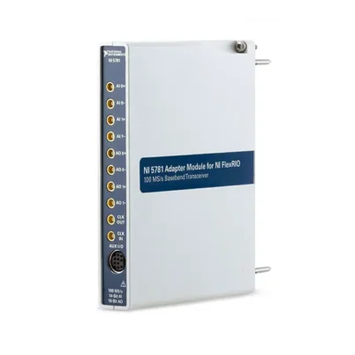
| NI-5781 | Baseband analog input and output | External RF conversion and baseband research |
Recommended Related Products
- NI-5792 RF Receiver Adapter
- NI-5791 RF Transceiver Adapter
- NI-5781 Baseband Transceiver Adapter
- PXIe-7966R FlexRIO FPGA Module
- View More NI RF and FlexRIO Modules
Frequently Asked Questions
What is the NI-5793?
The NI-5793 is an FPGA-programmable RF transmitter adapter covering frequencies from 200 MHz to 4.4 GHz.
What is its instantaneous bandwidth?
The specified instantaneous bandwidth is 200 MHz at 6 dB and 130 MHz at 3 dB.
What is the maximum nominal output power?
The RF output range extends from the noise floor to approximately +8 dBm nominal, depending on operating conditions and frequency.
Can the NI-5793 receive RF signals?
No. It is a transmitter adapter. Use the NI-5792 for receive-only applications or the NI-5791 when both functions are required.
Does it support external local-oscillator operation?
Yes. The module provides LO IN and LO OUT connections for synchronized RF configurations.
Is the NI-5793 a standalone signal generator?
No. It requires a compatible FlexRIO FPGA module or supported Controller for FlexRIO.
What is the NI-5793 part number?
The standard ordering part number is 782512-01.
Request a Quote for the NI-5793
Contact us for pricing, availability and configuration assistance for the NI-5793 200 MHz to 4.4 GHz RF Transmitter Adapter. We can also help select the FPGA carrier, RF cables and synchronization components.