






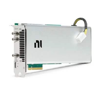
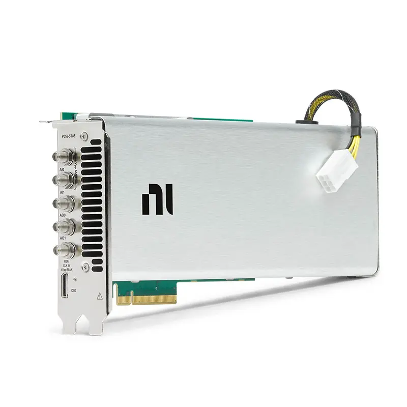
PCIe-5785 12-Bit 6.4 GS/s FlexRIO IF Transceiver
The PCIe-5785 is a high-performance PCI Express FlexRIO intermediate-frequency transceiver designed for direct RF acquisition, wideband waveform generation and FPGA-based real-time signal processing.
It combines two 12-bit analog input channels, two 12-bit analog output channels and a user-programmable Xilinx Kintex UltraScale FPGA on one integrated PCI Express card. The analog inputs acquire signals from approximately 500 kHz to 6 GHz, while the outputs generate signals with bandwidth up to 2.85 GHz, depending on operating mode and reconstruction-filter configuration.
The PCIe-5785 is well suited to radar prototyping, electronic warfare, communications research, software-defined radio, spectrum monitoring and other applications requiring synchronized wideband acquisition and generation.
Key Features of the PCIe-5785
- Two simultaneously sampled analog input channels
- Two simultaneously updated analog output channels
- 12-bit analog input and output resolution
- 3.2 GS/s per input channel in dual-channel mode
- 6.4 GS/s input sampling in single-channel interleaved mode
- 6.4 GS/s DAC update rate with 2× interpolation
- 500 kHz to 6 GHz analog input bandwidth
- Up to 2.85 GHz analog output bandwidth
- AC-coupled 50 Ω analog inputs and outputs
- 1.25 Vpp full-scale analog input range
- Optional analog-output reconstruction filters
- Kintex UltraScale KU035, KU040 or KU060 FPGA
- Up to 4 GB of onboard DRAM
- Eight bidirectional digital I/O channels
- High-speed multi-gigabit transceivers on supported FPGA versions
- External reference-clock and sample-clock support
- PCI Express Gen 3 x8 host interface
- FlexRIO driver and LabVIEW FPGA support
PCIe-5785 Technical Specifications
| Product Model | PCIe-5785 |
|---|---|
| Product Type | PCI Express FlexRIO IF transceiver device |
| Analog Input Channels | 2, single-ended and simultaneously sampled |
| Analog Output Channels | 2, single-ended and simultaneously updated |
| Analog Input Resolution | 12 bits |
| Analog Output Resolution | 12 bits |
| Analog-to-Digital Converter | ADC12DJ3200 |
| Digital-to-Analog Converter | DAC38RF82 |
| Dual-Channel Input Sample Rate | 3.2 GS/s per channel |
| Single-Channel Input Sample Rate | 6.4 GS/s, interleaved |
| Analog Output Update Rate | 6.4 GS/s with 2× interpolation |
| Dual-Channel Output Data Rate | 3.2 GS/s real per channel |
| Single-Channel Output Data Rate | 3.2 GS/s complex |
| Analog Input Bandwidth | 500 kHz to 6 GHz, -3 dB |
| Dual-Channel Output Bandwidth | 3 MHz to 1.53 GHz |
| Single-Channel Output Bandwidth without Filter | 60 MHz to 2.85 GHz |
| Single-Channel Output Bandwidth with Filter | 60 MHz to 2.35 GHz |
| Analog Input Coupling | AC |
| Analog Output Coupling | AC |
| Analog Input Impedance | 50 Ω |
| Analog Output Impedance | 50 Ω |
| Analog Input Range | 1.25 V peak-to-peak, 5.92 dBm at 10 MHz |
| Dual-Channel Full-Scale Output | 2.85 dBm, 878 mVpp into 50 Ω |
| Single-Channel Full-Scale Output | -3.33 dBm, 431 mVpp into 50 Ω |
| Analog I/O Connectors | Four SMA connectors: AI 0, AI 1, AO 0 and AO 1 |
| Internal Sample Clock | 3.2 GHz |
| External Sample Clock | 2.8 GHz to 3.2 GHz |
| External Reference Clock | 10 MHz |
| Measured Input Sample-Clock Jitter | 86.8 fs RMS |
| Measured Output Sample-Clock Jitter | 198.8 fs RMS |
| FPGA Options | Kintex UltraScale KU035, KU040 or KU060 |
| Onboard DRAM | 0 GB on KU035; 4 GB on KU040 and KU060 versions |
| Maximum Theoretical DRAM Rate | 17 GB/s on configurations with 4 GB DRAM |
| Single-Ended Digital I/O | 8 bidirectional channels |
| High-Speed Serial Interface | 4 transmit and 4 receive MGT lanes on supported FPGA configurations |
| Digital I/O Connector | Molex Nano-Pitch I/O |
| Bus Interface | PCI Express Gen 3 x8 |
| Compatible PCI Express Slots | x8 and x16 |
| Maximum Total Power | 75 W |
| Mechanical Format | Standard-height, three-quarter-length, double-slot card |
| Dimensions | 12.6 cm × 26.3 cm × 4.0 cm |
| Weight | 990 g |
| Operating Temperature | 0°C to 45°C at the fan inlet |
PCIe-5785 Part Number Options
| Part Number | FPGA | DRAM | Output Filter | Maximum Single-Channel Output Bandwidth |
|---|---|---|---|---|
| 785587-01 | Kintex UltraScale KU035 | 0 GB | No reconstruction filter | 2.85 GHz |
| 785587-02 | Kintex UltraScale KU035 | 0 GB | With reconstruction filter | 2.35 GHz |
| 785588-01 | Kintex UltraScale KU040 | 4 GB | No reconstruction filter | 2.85 GHz |
| 785588-02 | Kintex UltraScale KU040 | 4 GB | With reconstruction filter | 2.35 GHz |
| 785589-01 | Kintex UltraScale KU060 | 4 GB | No reconstruction filter | 2.85 GHz |
| 785589-02 | Kintex UltraScale KU060 | 4 GB | With reconstruction filter | 2.35 GHz |
The -01 configurations provide the widest analog output bandwidth and do not include an output reconstruction filter. The -02 configurations include the reconstruction filter, reducing the maximum output bandwidth while suppressing unwanted DAC images.
Integrated FlexRIO IF Transceiver Architecture
The PCIe-5785 integrates its analog input front end, ADC, analog output front end, DAC, FPGA and PCI Express interface on one card. The I/O assembly is permanently integrated and is not a removable or interchangeable FlexRIO adapter module.
No separate FlexRIO FPGA carrier is required. The selected KU035, KU040 or KU060 FPGA is included as part of the PCIe-5785 configuration.
Two Wideband Analog Inputs
The PCIe-5785 provides two single-ended analog inputs through standard SMA connectors. Both inputs are simultaneously sampled in dual-channel mode, preserving the timing and phase relationship between the acquired signals.
The input channels have a nominal impedance of 50 Ω and use AC-coupled signal paths. They are intended for wideband IF and RF signals rather than DC measurements.
Direct RF Acquisition to 6 GHz
The analog input path provides a typical -3 dB passband from 500 kHz to 6 GHz. This enables direct acquisition of many RF and intermediate-frequency signals without an external analog downconverter.
Signals above the first Nyquist zone can be intentionally undersampled when the source, band selection and alias mapping are correctly engineered. External filtering may be required to prevent unwanted spectral bands from folding into the acquisition bandwidth.
Dual-Channel 3.2 GS/s Input Mode
In dual-channel mode, the ADC simultaneously samples AI 0 and AI 1 at 3.2 GS/s per channel. This mode is suitable for phase-coherent receiver channels, antenna measurements and comparison of related RF signals.
Multi-channel synchronization allows the FPGA to perform phase comparison, correlation, beamforming and other algorithms that depend on a consistent relationship between the two acquired channels.
Single-Channel 6.4 GS/s Input Mode
In single-channel mode, the ADC cores are interleaved to achieve an aggregate rate of 6.4 GS/s on one channel. This produces twice the sample density available from one channel in dual-channel mode.
Interleaved operation is useful when maximum time resolution is required. Fixed interleaving spurs and channel-specific spectral performance should be considered when designing precision frequency-domain measurements.
1.25 Vpp Analog Input Range
The analog input has a typical full-scale range of 1.25 V peak-to-peak, corresponding to approximately 5.92 dBm into 50 Ω at 10 MHz.
External gain, attenuation or protection may be necessary to match the source level to the digitizer. Signal peaks must remain within the permitted input limits, including modulation peaks and unexpected transients.
Two Wideband Analog Outputs
The device provides two single-ended, simultaneously updated analog outputs through SMA connectors. Each output is AC coupled and has a nominal impedance of 50 Ω.
The outputs can generate wideband IF and RF waveforms for radar simulation, communications prototyping, receiver testing and closed-loop channel experiments.
6.4 GS/s DAC Update Rate
The output DAC operates with a 6.4 GS/s update rate when 2× interpolation is enabled. In dual-channel real-output mode, the data rate is 3.2 GS/s per channel.
A single-channel complex mode is also available with a 3.2 GS/s complex data rate. FPGA-based digital upconversion can translate a complex baseband waveform to a higher output frequency.
Analog Output Bandwidth
In dual-channel mode, the typical -3 dB output passband is 3 MHz to 1.53 GHz. In single-channel mode without the reconstruction filter, the output passband extends from approximately 60 MHz to 2.85 GHz.
Versions equipped with the reconstruction filter provide a typical single-channel passband from 60 MHz to 2.35 GHz. The filtered configuration reduces DAC image content at the expense of maximum output bandwidth.
Output Reconstruction Filter Options
The -02 part numbers include an analog reconstruction filter in each output path. This filter smooths the generated waveform and suppresses spectral images produced by the digital-to-analog conversion process.
The unfiltered -01 versions are appropriate when the application requires maximum bandwidth or when external filtering is provided. The -02 versions simplify applications that benefit from integrated image rejection within their required frequency band.
Analog Output Level
In dual-channel mode, the typical full-scale output is 2.85 dBm, equivalent to approximately 878 mV peak-to-peak into 50 Ω. In single-channel mode, the typical level is -3.33 dBm or approximately 431 mV peak-to-peak.
An external amplifier may be required when the receiving device needs more power. Any amplifier should provide sufficient bandwidth and linearity for the generated waveform.
12-Bit ADC and DAC Resolution
Both the ADC and DAC use 12-bit conversion. The input converter provides 4,096 theoretical amplitude levels, while the output converter uses 12-bit waveform samples to generate the requested signal.
Actual dynamic performance depends on signal frequency, clock quality, analog noise, FPGA processing and operating mode. Converter resolution should not be interpreted as the effective number of bits at every RF frequency.
Kintex UltraScale KU035 Configuration
The KU035 configuration provides the lowest-cost FPGA option for applications that do not require onboard DRAM or the additional resources of the larger FPGA models.
The KU035 PCIe-5785 versions contain no user DRAM. Continuous streaming and FPGA memory requirements must therefore be designed around internal FPGA memory and host transfers.
Kintex UltraScale KU040 Configuration
The KU040 configuration provides additional FPGA logic and DSP resources together with 4 GB of onboard DRAM. It is suited to real-time filtering, digital downconversion, digital upconversion and buffered waveform applications.
The KU040 also supports the available high-speed serial transceiver connections through the auxiliary digital I/O connector.
Kintex UltraScale KU060 Configuration
The KU060 is the largest FPGA option offered for the PCIe-5785. It supports more complex and more highly parallel signal-processing designs than the smaller FPGA configurations.
Its 4 GB of onboard DRAM is useful for deep waveform storage, burst capture, playback and algorithms requiring large working buffers.
4 GB Onboard DRAM
The KU040 and KU060 versions include 4 GB of DRAM arranged as two 2 GB banks. The memory can buffer acquired data, store generated waveforms and support custom FPGA processing.
The maximum theoretical aggregate DRAM transfer rate is 17 GB/s. Actual performance depends on FPGA implementation, access patterns and simultaneous data movement.
Real-Time FPGA Signal Processing
The integrated FPGA can process data directly between the ADC and DAC with deterministic timing. This supports applications requiring lower latency than a host-only software architecture can provide.
Possible FPGA algorithms include digital downconversion, channelization, filtering, decimation, interpolation, digital upconversion, waveform detection, pulse compression and custom modulation.
Closed-Loop Acquisition and Generation
Because the PCIe-5785 combines analog inputs and outputs with an FPGA, an acquired signal can influence a generated response without requiring every sample to pass through the host processor.
This architecture is useful for channel emulation, hardware-in-the-loop RF testing, adaptive waveform generation and real-time stimulus-response systems.
Reference and Sample Clock Options
The PCIe-5785 can use an internal clock, a 10 MHz reference clock or an external sample clock between 2.8 GHz and 3.2 GHz. The external clock is connected through the REF/CLK IN SMA connector.
When a 3.2 GHz external sample clock and 2× interpolation are used, the output DAC can operate at its 6.4 GS/s update rate. Clock amplitude, accuracy, duty cycle and phase noise must satisfy the official specifications.
Low-Jitter Clocking
The measured sample-clock jitter is 86.8 fs RMS for the analog input and 198.8 fs RMS for the analog output under the documented conditions.
Low jitter is essential for maintaining dynamic performance at high RF frequencies. Use a low-phase-noise clock source and high-quality 50 Ω cabling when external clocking is required.
Eight Bidirectional Digital I/O Channels
The auxiliary Molex Nano-Pitch connector provides eight single-ended bidirectional digital I/O channels. These lines can be used for triggering, equipment control, status monitoring and custom low-speed communication.
The FPGA controls the direction and behavior of these channels. External circuits must match the configured LVCMOS voltage family and electrical limits.
Multi-Gigabit Transceiver Connections
Supported FPGA configurations provide four high-speed serial transmit lanes and four receive lanes through the auxiliary connector. These MGT connections can communicate with compatible external FPGA or digital hardware.
Implementing a high-speed serial link requires suitable FPGA protocol logic, controlled-impedance connections and detailed signal-integrity analysis.
PCI Express Gen 3 x8 Interface
The PCIe-5785 uses a PCI Express Gen 3 x8 host interface and can be installed in a compatible x8 or x16 slot. The PCI Express connection transfers configuration, waveform and processed measurement data between the device and host computer.
The system must also provide a compatible six-pin PCI Express power connection because the card’s power requirements exceed what should be assumed from the slot alone.
Typical PCIe-5785 Applications
- Radar prototyping and target simulation
- Electronic warfare research
- Signal intelligence systems
- Software-defined radio development
- Wideband communications testing
- Direct RF signal acquisition
- Real-time spectrum analysis
- RF modulation and demodulation
- Digital downconversion and upconversion
- Channel emulation
- Pulse compression
- Custom RF hardware-in-the-loop testing
- Multi-channel phase-coherent measurements
- Wideband waveform playback
Radar Prototyping
The PCIe-5785 can acquire radar returns and generate test or stimulus waveforms using the same integrated FPGA platform. FPGA logic can perform pulse detection, digital downconversion, filtering and other radar-processing functions.
External RF amplification, attenuation, switching and protection may be required to interface with the complete radar signal chain.
Electronic Warfare and Signal Intelligence
The 500 kHz to 6 GHz input passband supports wideband monitoring and direct acquisition of many signals of interest. FPGA algorithms can detect events, channelize spectrum and reduce raw data before transferring results to the host.
The device is a component for authorized measurement and research systems. Deployment must follow applicable radio-frequency, privacy, export-control and spectrum-use requirements.
Communications Research
The two inputs and outputs support development of custom transmit-and-receive algorithms for wideband communications. The FPGA can perform modulation, demodulation, synchronization and real-time protocol processing.
The selectable reconstruction-filter option allows the output architecture to prioritize either maximum analog bandwidth or improved suppression of unwanted DAC images.
Channel Emulation
The FPGA can receive an input signal, apply a mathematical channel model and generate a modified output signal. Possible effects include delay, attenuation, filtering and other deterministic transformations.
The achievable model complexity and latency depend on FPGA resources, memory use, sample-rate processing architecture and the selected KU035, KU040 or KU060 configuration.
FlexRIO Driver Support
The NI FlexRIO driver includes support for acquiring and generating waveforms without requiring every function to be developed from the beginning. This provides a practical starting point for device evaluation and standard streaming applications.
Engineers can then develop custom FPGA logic when the application requires specialized signal processing, nonstandard triggering or deterministic input-to-output behavior.
LabVIEW FPGA Programming
LabVIEW FPGA can be used to program the Kintex UltraScale FPGA. The graphical development environment supports parallel, deterministic processing and access to the device’s ADC, DAC, DRAM, digital I/O and clocking resources.
Changing the FPGA design requires compilation. Resource use, timing closure and compilation time depend on the selected FPGA and the complexity of the processing architecture.
Computer and Cooling Requirements
The PCIe-5785 is a standard-height, three-quarter-length, double-slot PCI Express card. The host computer must provide sufficient internal length, two-slot clearance, an x8 or x16 PCI Express slot and the required auxiliary power connector.
The card includes an integrated fan. Keep its inlet and exhaust paths unobstructed and maintain the local fan-inlet temperature between 0°C and 45°C.
PCIe-5785 Troubleshooting
The PCIe-5785 is not detected
Confirm that the device is fully inserted into a compatible PCI Express x8 or x16 slot. Check the six-pin auxiliary power connection, FlexRIO driver installation, operating-system compatibility and computer firmware settings.
The analog input contains no DC component
This is expected because the PCIe-5785 analog inputs are AC coupled. Select a DC-coupled digitizer such as the PCIe-5774 when DC and low-frequency content must be preserved.
The input signal is clipped
Reduce the input level or add an external attenuator. Include modulation peaks and transient amplitude when comparing the signal with the 1.25 Vpp full-scale input range.
The generated output level is lower than expected
Confirm whether the device is operating in dual-channel or single-channel mode. The typical full-scale output levels differ between these configurations.
The output bandwidth is limited to approximately 2.35 GHz
Check the product part number. The -02 versions contain output reconstruction filters and have a lower maximum passband than the unfiltered -01 versions.
The generated waveform contains unwanted images
Use a -02 reconstruction-filter configuration or install suitable external filtering. Also verify the DAC interpolation, inverse-sinc and digital-upconversion settings.
The external sample clock does not lock
Confirm that the external clock is between 2.8 GHz and 3.2 GHz and satisfies the required amplitude, impedance, duty-cycle and jitter specifications.
The device does not have onboard DRAM
KU035 configurations contain 0 GB of DRAM. Select a KU040 or KU060 part number when the FPGA application requires 4 GB of onboard memory.
The FPGA design does not compile
Review FPGA resource usage and timing constraints. Reduce processing parallelism, pipeline long paths or select a configuration with a larger KU040 or KU060 FPGA.
The device overheats
Check the integrated fan, computer airflow, adjacent-slot clearance and cable placement. The local air temperature at the fan inlet must remain within the operating limit.
PCIe-5785 Comparison with Similar FlexRIO Devices
| Model | Primary Configuration | Best Suited For |
|---|---|---|
| PCIe-5785 | 2 AI, 2 AO, 12 bits, 6.4 GS/s input, AC coupled | Integrated wideband RF acquisition and generation |
| PXIe-5785 | 2 AI, 2 AO, 12 bits, 6.4 GS/s input, AC coupled | Wideband transceiver applications in PXI Express systems |
| PCIe-5775 | 2 AI, 12 bits, 6.4 GS/s, 6 GHz AC-coupled bandwidth | Wideband acquisition without analog generation |
| PCIe-5774 | 2 AI, 12 bits, 6.4 GS/s, DC coupled | Time-domain acquisition requiring DC response |
| PXIe-5745 | 2 AO, 12 bits, 6.4 GS/s update rate | PXI Express applications requiring waveform generation only |
PCIe-5785 vs PCIe-5775
The PCIe-5785 combines two analog inputs and two analog outputs, while the PCIe-5775 is an input-only digitizer. Both support 12-bit acquisition and a maximum single-channel input sample rate of 6.4 GS/s.
Choose the PCIe-5785 for transceiver, closed-loop or waveform-generation applications. Choose the PCIe-5775 when only wideband acquisition is required.
PCIe-5785 vs PCIe-5774
The PCIe-5785 uses AC-coupled inputs with a passband extending to 6 GHz and includes two analog outputs. The PCIe-5774 uses DC-coupled inputs with up to approximately 3 GHz of analog bandwidth and does not provide analog waveform outputs.
Choose the PCIe-5785 for direct RF transceiver applications. Choose the PCIe-5774 for high-speed time-domain measurements that must preserve DC and low-frequency content.
PCIe-5785 vs PXIe-5785
The PCIe-5785 installs directly in a compatible workstation or industrial computer. The PXIe-5785 provides similar transceiver functionality in a PXI Express module.
Select the PCIe model for a computer-based custom instrument. Select the PXIe-5785 when the test system requires PXI synchronization, modular instrumentation and chassis-based integration.
Recommended Related Products
- PXIe-5785 12-Bit 6.4 GS/s FlexRIO IF Transceiver
- PCIe-5775 12-Bit 6.4 GS/s FlexRIO Digitizer
- PXIe-5775 12-Bit 6.4 GS/s FlexRIO Digitizer
- PCIe-5774 12-Bit 6.4 GS/s DC-Coupled FlexRIO Digitizer
- PXIe-5745 12-Bit 6.4 GS/s FlexRIO Signal Generator
- View More NI FlexRIO Products
- View More NI PCI and USB Data Acquisition Products
Selecting the Right PCIe-5785 Configuration
Select a KU035 configuration for applications that do not require onboard DRAM and can fit within the smaller FPGA. Choose KU040 or KU060 when the application requires 4 GB of DRAM, additional processing resources or supported high-speed serial connectivity.
Choose a -01 part number for maximum analog output bandwidth. Select a -02 part number when integrated reconstruction filtering and improved suppression of unwanted output images are more important than maximum bandwidth.
Why Choose the PCIe-5785?
- Combines wideband RF acquisition and generation
- Provides two synchronized input and output channels
- Acquires signals directly up to 6 GHz
- Generates signals with bandwidth up to 2.85 GHz
- Provides 12-bit input and output resolution
- Supports 6.4 GS/s interleaved input sampling
- Includes a programmable Kintex UltraScale FPGA
- Offers filtered and unfiltered output configurations
- Provides up to 4 GB of onboard DRAM
- Supports deterministic real-time signal processing
- Offers external clock and digital I/O connectivity
- Installs directly in a PCI Express workstation
Frequently Asked Questions
What is the PCIe-5785?
The PCIe-5785 is a two-input, two-output, 12-bit PCI Express FlexRIO IF transceiver for wideband RF acquisition, waveform generation and FPGA signal processing.
How many analog channels does it provide?
It provides two analog input channels and two analog output channels.
What is the maximum input sample rate?
The maximum input rate is 6.4 GS/s in single-channel interleaved mode. Both channels can be simultaneously sampled at 3.2 GS/s per channel.
What is the analog input bandwidth?
The typical -3 dB analog input passband extends from 500 kHz to 6 GHz.
What is the analog output bandwidth?
The unfiltered -01 versions provide up to approximately 2.85 GHz in single-channel mode. Filtered -02 versions provide up to approximately 2.35 GHz.
Are the inputs and outputs AC or DC coupled?
Both the analog inputs and analog outputs are AC coupled with a nominal impedance of 50 Ω.
What FPGA options are available?
The available FPGA options are the Xilinx Kintex UltraScale KU035, KU040 and KU060.
Which versions include onboard DRAM?
The KU040 and KU060 configurations include 4 GB of DRAM. KU035 configurations have no onboard DRAM.
What is the difference between -01 and -02 part numbers?
The -01 versions do not include the output reconstruction filter and provide greater output bandwidth. The -02 versions include the filter for improved DAC image suppression.
Does the PCIe-5785 require a separate FPGA carrier?
No. It is an integrated device containing the ADCs, DACs, FPGA and PCI Express interface on one card.
Can it acquire and generate signals at the same time?
Yes. Its integrated input, output and FPGA architecture supports simultaneous acquisition, generation and custom real-time processing.
Can it use an external sample clock?
Yes. The REF/CLK IN connector accepts an external sample clock between 2.8 GHz and 3.2 GHz or a supported external reference clock.
Which PCI Express slots are compatible?
The PCIe-5785 uses a PCI Express Gen 3 x8 interface and can be installed in compatible x8 or x16 slots.
Does it require auxiliary power?
Yes. Installation requires the appropriate six-pin PCI Express power connection in addition to the card-edge interface.
What are the PCIe-5785 part numbers?
The available part numbers are 785587-01, 785587-02, 785588-01, 785588-02, 785589-01 and 785589-02.
Request a Quote for the PCIe-5785
Contact us for current availability, lead time and project pricing for the PCIe-5785 12-Bit 6.4 GS/s FlexRIO IF Transceiver. Please provide the required FPGA, onboard-memory and reconstruction-filter configuration so we can confirm the correct part number.















