






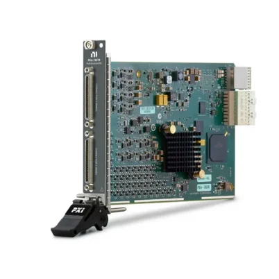
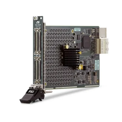
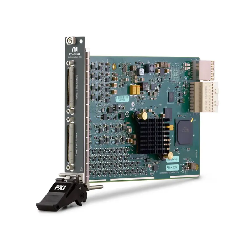
PXIe-7858 Kintex-7 325T FPGA Multifunction RIO Module
The PXIe-7858 is a high-performance PXI Express multifunction reconfigurable I/O module featuring a user-programmable Kintex-7 325T FPGA. It combines analog input, analog output, digital I/O and onboard DRAM in a single module for advanced test, measurement and control systems.
With 8 analog inputs, 8 analog outputs, 48 bidirectional digital I/O lines and sampling rates up to 1 MS/s per analog channel, the PXIe-7858 is well suited for hardware-in-the-loop testing, custom protocol implementation, sensor simulation and high-speed closed-loop control.
Key Features of the PXIe-7858
- Kintex-7 325T user-programmable FPGA
- 512 MB onboard DRAM
- 8 simultaneously sampled analog input channels
- 16-bit analog input resolution
- 1 MS/s maximum sampling rate per analog input
- 8 analog output channels with 16-bit resolution
- 1 MS/s maximum update rate per analog output
- 48 bidirectional digital I/O lines
- Maximum digital clock rate of 80 MHz
- Selectable 1.2 V, 1.5 V, 1.8 V, 2.5 V and 3.3 V digital logic
- Independent timing and triggering for individual channels
- Support for multirate sampling and custom FPGA processing
- PXI peer-to-peer data streaming support
PXIe-7858 Technical Specifications
| Product Model | PXIe-7858 |
|---|---|
| Part Number | 784147-01 |
| Product Type | PXI Express Multifunction Reconfigurable I/O Module |
| FPGA | Kintex-7 325T |
| Onboard Memory | 512 MB DRAM |
| Analog Inputs | 8 |
| Analog Input Resolution | 16 bit |
| Maximum Analog Input Rate | 1 MS/s per channel |
| Analog Input Ranges | ±1 V, ±2 V, ±5 V and ±10 V |
| Analog Outputs | 8 |
| Analog Output Resolution | 16 bit |
| Maximum Analog Output Rate | 1 MS/s per channel |
| Analog Output Range | ±10 V |
| Digital I/O | 48 bidirectional lines |
| Maximum Digital Clock Rate | 80 MHz |
| Digital Logic Levels | 1.2 V, 1.5 V, 1.8 V, 2.5 V and 3.3 V |
| Bus Type | PXI Express |
| Front Connectors | 2 × 68-pin VHDCI |
| Operating Temperature | 0°C to 55°C |
PXIe-7858 Part Number and Accessories
| Item | Part Number | Description |
|---|---|---|
| PXIe-7858 | 784147-01 | Kintex-7 325T FPGA multifunction RIO module with 512 MB DRAM |
| SCB-68 HSDIO | 782914-01 | Shielded 68-pin digital I/O connector block |
| SCB-68A | 782536-01 | Shielded screw-terminal connector block |
| SHC68-C68-RDIO2 | 156166-02 | 2 m shielded 68-pin digital I/O cable |
| SHC68-NT-S | 189041-02 | 2 m shielded cable with unterminated leads |
Cable and terminal block requirements depend on the analog and digital signals used in the application. Confirm connector compatibility before ordering accessories.
Kintex-7 325T FPGA Processing
The PXIe-7858 uses a larger Kintex-7 325T FPGA to execute custom measurement, timing, triggering and control logic directly in hardware. Compared with modules based on the Kintex-7 160T FPGA, it provides additional FPGA capacity for more complex algorithms and parallel processing.
Engineers can implement custom communication protocols, inline signal processing, high-speed feedback loops and application-specific triggering without relying exclusively on host-computer software.
512 MB Onboard DRAM
The module includes 512 MB of onboard DRAM for waveform buffering, data logging and FPGA-based processing. This memory is useful when data must be stored temporarily before transfer to the PXI controller or processed in blocks directly by the FPGA.
The combination of a larger FPGA and onboard memory makes the PXIe-7858 suitable for demanding applications involving long waveform records, high-throughput data movement or memory-intensive processing.
Simultaneous Analog Input Acquisition
Each of the eight analog input channels uses a dedicated 16-bit analog-to-digital converter. The channels can therefore acquire signals simultaneously at rates up to 1 MS/s per channel, avoiding the timing skew associated with multiplexed measurement architectures.
Independent channel timing allows different sampling rates and triggering conditions to be implemented for individual signals through the FPGA.
Programmable Analog Input Ranges
The PXIe-7858 supports programmable analog input ranges of ±1 V, ±2 V, ±5 V and ±10 V. Selecting the appropriate range helps improve measurement resolution for both low-level and higher-voltage signals.
Differential, referenced single-ended and nonreferenced single-ended input configurations can be used according to the grounding and noise requirements of the system.
High-Speed Analog Output Generation
The module provides eight 16-bit analog output channels with update rates up to 1 MS/s per channel. These outputs can generate control signals, simulated sensor waveforms and deterministic responses controlled directly by FPGA logic.
Because the outputs are FPGA-timed, the PXIe-7858 can maintain precise relationships between analog acquisition, waveform generation and digital events.
48 Bidirectional Digital I/O Lines
The PXIe-7858 includes 48 bidirectional digital I/O lines. Its high-speed digital lines support clock rates up to 80 MHz, while the direction and behavior of individual lines can be defined by the FPGA application.
Selectable logic levels of 1.2 V, 1.5 V, 1.8 V, 2.5 V and 3.3 V simplify integration with embedded controllers, digital interfaces, sensors and custom electronic devices.
Independent Timing and Triggering
Unlike fixed-function data acquisition devices, the PXIe-7858 allows timing and triggering behavior to be created in FPGA hardware. Analog and digital channels can operate at different rates while maintaining deterministic synchronization.
This flexibility is particularly valuable for applications that require custom trigger qualification, event sequencing, pulse generation or low-latency responses.
PXI Peer-to-Peer Streaming
PXI peer-to-peer streaming allows supported modules to exchange data directly across the PXI Express backplane. This can reduce host processor involvement and lower data-transfer latency in high-performance test systems.
Compatibility should be verified for the selected PXI chassis, controller and peer-to-peer modules before system integration.
Typical Applications
- Hardware-in-the-loop simulation
- High-speed closed-loop control
- Custom digital protocol implementation
- Sensor and actuator simulation
- Power electronics testing
- Motor and inverter control
- Automotive electronic control unit testing
- FPGA-based signal processing
- Semiconductor and component validation
- Automated production testing
LabVIEW FPGA Programming
The PXIe-7858 is programmed using the LabVIEW FPGA Module and a compatible NI RIO driver environment. Developers can create custom FPGA personalities for acquisition, generation, triggering, communication and real-time processing.
Compiled FPGA applications run independently of the host operating system, providing deterministic execution and predictable response times for time-critical operations.
Connectivity and Signal Wiring
Two 68-pin VHDCI connectors provide access to the analog and digital signals. Compatible shielded cables and terminal blocks help simplify connection to test fixtures, devices under test and external signal-conditioning hardware.
For reliable performance, use appropriate shielding, grounding and impedance-control practices, particularly when working with high-speed digital signals or low-level analog measurements.
PXI Express System Integration
The PXIe-7858 requires a compatible PXI Express chassis and controller. Chassis selection should account for slot compatibility, cooling capacity, backplane bandwidth, synchronization requirements and the total power consumption of all installed modules.
Visit the NI PXI Modules category to explore compatible PXI hardware and related measurement products.
Troubleshooting the PXIe-7858
The module is not detected by the system
Verify that the module is installed in a compatible PXI Express slot. Check the PXI Platform Services, RIO driver installation and chassis controller configuration.
The FPGA application cannot be compiled or downloaded
Confirm that the installed LabVIEW FPGA and driver versions support the PXIe-7858. Also verify that the FPGA bitfile was compiled specifically for this module.
Analog measurements contain excessive noise
Check signal grounding, shielding, cable routing and input configuration. Use the smallest appropriate input range and avoid routing sensitive analog wiring near high-speed digital or power cables.
Digital signals are not recognized correctly
Verify that the selected digital logic voltage matches the connected device. Confirm the FPGA line direction, connector pin assignment and external grounding.
Data transfer performance is lower than expected
Review DMA FIFO configuration, onboard DRAM buffering, host processing load and PXI Express bandwidth. Peer-to-peer streaming may improve performance in supported systems.
PXIe-7858 Comparison
| Model | FPGA | Analog Rate | DRAM | I/O Configuration |
|---|---|---|---|---|
| PXIe-7858 | Kintex-7 325T | 1 MS/s | 512 MB | 8 AI, 8 AO, 48 DIO |
| PXIe-7857 | Kintex-7 160T | 1 MS/s | 512 MB | 8 AI, 8 AO, 48 DIO |
| PXIe-7856 | Kintex-7 160T | 1 MS/s | No onboard DRAM | 8 AI, 8 AO, 48 DIO |
| PXIe-7846 | Kintex-7 160T | 500 kS/s | No onboard DRAM | 8 AI, 8 AO, 48 DIO |
Recommended Related Products
- PXIe-7857 – 1 MS/s multifunction RIO module with a Kintex-7 160T FPGA and 512 MB DRAM
- PXIe-7856 – 1 MS/s multifunction RIO module without onboard DRAM
- PXIe-7846 – 500 kS/s multifunction RIO module for less demanding applications
- PXIe-7820 – FPGA-based digital RIO module for custom digital interfaces
- PXIe-1092 – PXI Express chassis for modular test and measurement systems
Selecting the PXIe-7858
Choose the PXIe-7858 when your application requires simultaneous analog acquisition, analog generation, high-speed digital I/O, onboard waveform memory and substantial FPGA processing capacity.
If the same I/O configuration and DRAM capacity are required but the FPGA design is less complex, the PXIe-7857 may provide a more economical alternative. Applications that do not require onboard DRAM can consider the PXIe-7856.
PXIe-7858 vs PXIe-7857
The PXIe-7858 and PXIe-7857 both provide 8 analog inputs, 8 analog outputs, 48 digital I/O lines, 1 MS/s analog operation and 512 MB of onboard DRAM.
The primary difference is FPGA capacity. The PXIe-7858 uses a Kintex-7 325T FPGA, while the PXIe-7857 uses a Kintex-7 160T FPGA. The PXIe-7858 is therefore better suited to larger FPGA designs, more parallel processing and complex custom protocols.
Why Choose the PXIe-7858?
- Larger Kintex-7 325T FPGA for complex custom designs
- 512 MB DRAM for buffering and memory-intensive processing
- Simultaneous analog input sampling at up to 1 MS/s per channel
- Integrated analog output and high-speed digital I/O
- Deterministic FPGA-based timing and control
- Flexible logic voltage support for device interfacing
- PXI Express integration for modular automated test systems
Frequently Asked Questions
What is the PXIe-7858 used for?
The PXIe-7858 is used for FPGA-based measurement, hardware-in-the-loop testing, custom protocol implementation, sensor simulation and deterministic high-speed control.
Which FPGA does the PXIe-7858 use?
It uses a user-programmable Kintex-7 325T FPGA.
How much onboard memory does the PXIe-7858 provide?
The module includes 512 MB of onboard DRAM.
How many analog channels are available?
The PXIe-7858 provides eight analog input channels and eight analog output channels, all with 16-bit resolution.
What is the maximum analog sampling rate?
The eight analog inputs can be sampled simultaneously at rates up to 1 MS/s per channel.
How many digital I/O lines does the module have?
It provides 48 bidirectional digital I/O lines with a maximum digital clock rate of 80 MHz.
What is the difference between the PXIe-7858 and PXIe-7857?
The PXIe-7858 uses a larger Kintex-7 325T FPGA, while the PXIe-7857 uses a Kintex-7 160T FPGA. Their principal analog, digital and DRAM configurations are otherwise similar.
Can the PXIe-7858 operate without a PXI chassis?
No. It must be installed in a compatible PXI Express chassis and used with an appropriate controller and software environment.
What is the part number for the PXIe-7858?
The standard NI part number for the PXIe-7858 is 784147-01.
Request a Quote for the PXIe-7858
Contact us for current availability, lead time and project pricing for the PXIe-7858 Multifunction Reconfigurable I/O Module. We can also help confirm compatible PXI chassis, controllers, cables and terminal accessories for your application.















