






PXIe-2790 6 GHz Dual 2×1 RF Switch and Power Combiner
The PXIe-2790 is a solid-state PXI Express RF switch and power combiner designed for multi-device cellular, wireless-connectivity and production-test systems. It routes or combines RF signals from 10 MHz to 6 GHz through two independently controlled switching banks.
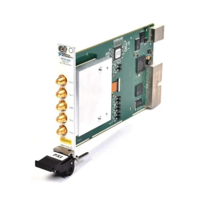
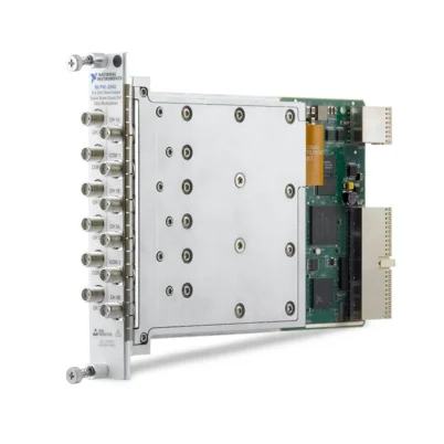
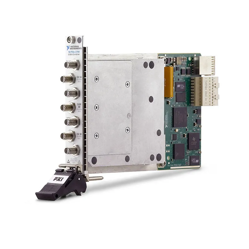
The module uses solid-state FET technology to provide fast switching without mechanical relay-contact wear. Seven front-panel SMA connectors provide access to Bank A, Bank B and the shared SUM AB power-combiner path.
Its combination of dual 2×1 switching, RF power combining, 50 Ω impedance and software-controlled routing allows multiple devices under test to share signal generators and RF analyzers while reducing the number of external switches and combiners required by the test fixture.
Key Features of the PXIe-2790
- Dual 2×1 RF multiplexer architecture
- Integrated solid-state RF power-combiner path
- Two independently controlled RF switching banks
- 10 MHz to 6 GHz operating frequency range
- 50 Ω nominal characteristic impedance
- AC-coupled signal paths
- Solid-state FET switching
- No mechanical relay-contact wear
- 45 µs maximum switching time
- +20 dBm maximum safe RF power on standard ports
- +30 dBm maximum safe RF power on the SUM AB port with chassis power on
- ±5 V maximum safe DC input voltage
- Greater than 31 dBm minimum input 1 dB compression point
- Fast multi-DUT RF routing
- Seven female SMA front-panel connectors
- PXI trigger-line support
- Programmable output-trigger pulse width
- NI-SWITCH software support
- NI Switch Executive compatibility
- Single-slot 3U PXI Express module
PXIe-2790 Technical Specifications
| Product Model | PXIe-2790 |
|---|---|
| Part Number | 782576-01 |
| Product Type | PXI Express RF multiplexer, switch and power combiner |
| Topology | Dual 2×1 switching banks with shared SUM AB power-combiner path |
| Software Topology Name | 2790/Independent |
| Switching Banks | Bank A and Bank B |
| Minimum Input Frequency | 10 MHz |
| Maximum Input Frequency | 6 GHz |
| Characteristic Impedance | 50 Ω nominal |
| Signal Coupling | AC |
| Switch Type | Solid-state FET |
| Maximum Safe DC Input Voltage | ±5 V |
| Maximum Safe RF Power, Standard Ports | +20 dBm with chassis power on |
| Maximum Safe RF Power, SUM AB | +30 dBm with chassis power on |
| Maximum Safe RF Power, Chassis Off | +20 dBm on all ports |
| COM-to-SUM Insertion Loss through 850 MHz | Less than 13.1 dB; less than 11.8 dB typical |
| COM-to-SUM Insertion Loss through 1.85 GHz | Less than 13.5 dB; less than 12.2 dB typical |
| COM-to-SUM Insertion Loss through 6 GHz | Less than 14.4 dB; less than 13.3 dB typical |
| COM-to-CH1 Insertion Loss through 850 MHz | Less than 2.3 dB; less than 1.2 dB typical |
| COM-to-CH1 Insertion Loss through 1.85 GHz | Less than 2.8 dB; less than 1.6 dB typical |
| COM-to-CH1 Insertion Loss through 6 GHz | Less than 3.8 dB; less than 2.8 dB typical |
| Bank-to-Bank COM Isolation | Greater than 19.6 dB specified through 6 GHz |
| CH1A-to-SUM AB Isolation through 850 MHz | Greater than 77 dB; greater than 82 dB typical |
| CH1A-to-SUM AB Isolation through 1.85 GHz | Greater than 68 dB; greater than 70 dB typical |
| CH1A-to-SUM AB Isolation through 6 GHz | Greater than 48.1 dB; greater than 51 dB typical |
| CH1A-to-CH1B Isolation through 6 GHz | Greater than 59.3 dB; greater than 62 dB typical |
| Input 1 dB Compression | Greater than 31 dBm minimum; greater than 33 dBm typical |
| Maximum Switch Operate Time | 45 µs |
| Input Trigger Sources | PXI trigger lines 0 through 7 |
| Minimum Trigger Pulse Width | 150 ns |
| Output Trigger Destinations | PXI trigger lines 0 through 7 |
| Output Trigger Pulse Width | Programmable from 1 µs to 62 µs |
| Front-Panel Connectors | 7 female SMA jacks |
| Power Requirement | 0.9 W at 3.3 V and 0.6 W at 12 V |
| Operating Temperature | 0°C to 55°C |
| Storage Temperature | -20°C to 70°C |
| Dimensions | 21.6 cm × 2.0 cm × 13.0 cm |
| Weight | 394 g |
| Bus Interface | PXI Express |
| Module Format | 3U, single-slot PXI Express module |
| Software Support | NI-SWITCH and NI Switch Executive |
| Life-Cycle Status | Discontinued |
PXIe-2790 Part Number and Accessories
| Item | Part Number | Description |
|---|---|---|
| PXIe-2790 | 782576-01 | 10 MHz to 6 GHz solid-state RF switch and power-combiner module |
| SMA 100 Cable | 763443-01 | 0.15 m flexible SMA male-to-SMA male RF cable |
| SMA 100 Cable | 763444-01 | 0.45 m flexible SMA male-to-SMA male RF cable |
| 50 Ω SMA Termination Plug | 778353-01 | Terminates unused PXIe-2790 RF ports |
| RF Torque Screwdriver and SMA Bit | 780895-01 | Tool kit for applying the recommended torque to SMA connections |
| RF SMA Driver Bit | 780894-01 | SMA driver bit for compatible torque tools |
The PXIe-2790 RF specifications assume that unused front-panel connectors are terminated with suitable 50 Ω loads. Confirm the required number of cables, termination plugs and adapters before ordering the module.
Dual 2×1 RF Switching Architecture
The PXIe-2790 contains two independently controlled RF banks identified as Bank A and Bank B. Each bank provides a common connection and alternative RF routes.
Independent control allows two DUT paths to be switched simultaneously. This is useful in multi-device production systems where separate RF paths must share generators, analyzers or a combined measurement connection.
Software should disconnect the active route in a bank before connecting an alternative path. This prevents unintended simultaneous connections and maintains the defined topology.
Integrated RF Power Combiner
The SUM AB port provides a shared path that combines signals associated with Bank A and Bank B. The combined signal can be routed to a common analyzer or measurement receiver.
This integrated combiner reduces the need for a separate external RF power combiner in multi-DUT fixtures. It can simplify cabling and make path calibration easier to manage within the automated test system.
Power-combiner paths have substantially more insertion loss than the direct COM-to-channel paths. The complete loss must be included when calculating the signal level delivered to the analyzer.
Independent Bank Operation
Bank A and Bank B can operate independently. A test application can route one bank to a direct channel while the other bank uses a separate route or participates in the combined path.
The initial hardware configuration connects SUM AB to COM A and SUM AB to COM B. Software can disconnect these paths and route the individual banks according to the required test sequence.
10 MHz to 6 GHz Frequency Range
The PXIe-2790 operates from 10 MHz to 6 GHz. This range covers many cellular, wireless LAN, Bluetooth, GNSS, industrial radio and general RF production-test applications.
The signal path is AC coupled and should not be used for DC routing. Select a DC-capable switch module if the test signal includes a required DC component or extends below 10 MHz.
50 Ω Terminated Signal Paths
The switch and power-combiner paths use a nominal 50 Ω characteristic impedance. Proper termination minimizes RF reflections and helps preserve the expected insertion loss, isolation and VSWR.
Unused ports should be fitted with 50 Ω terminations. Unterminated ports can change the response of the combiner and create reflections that affect measurement accuracy.
Solid-State FET Switching
The PXIe-2790 uses solid-state FET switches instead of electromechanical relay contacts. This architecture provides fast switching and does not have a mechanical contact-cycle limitation.
Solid-state technology is especially useful in high-volume production testing, where switching operations may occur continuously throughout the working day.
FET switches have different insertion-loss, isolation, compression and DC characteristics from electromechanical relays. These specifications should be evaluated against the required RF signal.
45 µs Switching Time
The maximum switch operate time is 45 µs. Fast route changes help reduce overhead in systems that alternate rapidly between multiple DUTs.
The complete measurement cycle may require additional settling time for the RF generator, analyzer, device under test or external fixture. Validate the finished system before selecting the minimum delay between switching and measurement.
Direct Channel Insertion Loss
The direct COM A-to-CH1A and COM B-to-CH1B paths specify insertion loss below 2.3 dB through 850 MHz, below 2.8 dB through 1.85 GHz and below 3.8 dB through 6 GHz.
Typical performance is below 2.8 dB at the upper frequency limit. External SMA cables, adapters and fixture traces add additional loss.
Power-Combiner Path Loss
The COM-to-SUM AB power-combiner path has higher loss because power is divided and combined within the RF network. Specified loss is below 13.1 dB through 850 MHz, below 13.5 dB through 1.85 GHz and below 14.4 dB through 6 GHz.
Test software should maintain different path-loss corrections for direct switching and combined operation. Using one correction value for both paths can produce large RF power errors.
Isolation Performance
Isolation between CH1 and SUM AB remains greater than 48.1 dB through 6 GHz, while isolation between CH1A and CH1B remains greater than 59.3 dB through 6 GHz.
High isolation helps prevent a strong signal from one DUT leaking into the measurement path of another DUT. External cable coupling and fixture design can still limit overall system isolation.
RF Compression and Linearity
The PXIe-2790 minimum input 1 dB compression point is greater than 31 dBm, with typical performance above 33 dBm. This provides useful linear operating margin for common cellular and wireless production-test signal levels.
Safe-input power and compression are different limits. For normal operation, the signal must satisfy the safe-power rating of the specific port and remain low enough to meet the required linearity.
RF Power Handling
With chassis power on, COM A, COM B and the individual channel ports accept maximum safe continuous RF power of +20 dBm. SUM AB accepts as much as +30 dBm.
When chassis power is off, every port is limited to +20 dBm. Remove or reduce the RF signal before shutting down the PXI Express chassis.
Maximum Safe DC Input
The maximum safe DC voltage on any RF port is ±5 V. Because the signal paths are AC coupled, the module is intended for RF rather than DC switching.
Install a suitable external DC block when a connected DUT or instrument can apply an unsafe DC level to the PXIe-2790.
Front-Panel SMA Connections
The PXIe-2790 provides seven female SMA connectors: COM A, COM B, the individual Bank A and Bank B channel connections, and SUM AB.
Use 50 Ω SMA cables rated through at least 6 GHz. Apply the recommended connector torque using an appropriate torque screwdriver to maintain repeatable insertion loss and return loss.
PXI Hardware Triggering
Input triggers can be received from PXI trigger lines 0 through 7. The normal minimum recognized trigger pulse width is 150 ns, although shorter pulses may be recognized when digital filtering is disabled.
Output triggers can be routed to PXI trigger lines 0 through 7 with a programmable pulse width from 1 µs to 62 µs. Hardware triggering allows switching events to be synchronized with RF generators, analyzers and production handlers.
RF Path Calibration
Multi-DUT systems should store individual calibration information for each PXIe-2790 route. Direct paths and combined paths have different insertion loss, and external cable loss can vary from port to port.
Calibrate the complete route from the generator or DUT reference plane to the analyzer connection. Recalibration may be required after changing cables, fixtures, adapters or switch modules.
Typical PXIe-2790 Applications
- Multi-DUT cellular production testing
- Wireless-connectivity device testing
- Bluetooth and WLAN validation
- RF signal switching and power combining
- Parallel receiver testing
- Transmitter output routing
- RF analyzer input sharing
- Signal-generator distribution
- Automated manufacturing test
- RF semiconductor testing
- Multi-site fixture routing
- Research and laboratory automation
Multi-DUT Cellular Testing
The PXIe-2790 was designed for production systems testing multiple cellular devices. Separate Bank A and Bank B connections can route signals for two DUT paths, while SUM AB allows selected signals to share a receiving instrument.
Fast solid-state switching helps reduce the routing delay between devices. Individual path correction maintains accurate RF power at every DUT and analyzer reference plane.
Wireless-Connectivity Production Test
The 6 GHz upper frequency supports many Bluetooth, WLAN and other wireless-connectivity bands. The module can switch RF stimulus between multiple devices or combine responses for an appropriate test architecture.
Use shielding and high-isolation fixtures to prevent over-the-air coupling from bypassing the intended switch route.
Analyzer Input Sharing
Multiple DUT outputs can share one spectrum analyzer or vector signal analyzer through the PXIe-2790. Test software selects the required direct or combined route before beginning the measurement.
Confirm that the total power applied to the analyzer remains within its input limits, especially when using SUM AB to combine two active signals.
RF Generator Routing
An RF generator can be routed between separate DUT paths without manual cable changes. This allows one generator to serve multiple fixture locations in an automated sequence.
The generator level should include compensation for the selected switch path, cables and adapters. Direct and combined routes require different correction values.
RF Semiconductor Testing
The module can route RF stimulus and response signals among multiple RFIC sites or load-board connections. Fast switching and freedom from mechanical contact wear are valuable in high-volume semiconductor test systems.
Protect every switch port from electrostatic discharge, unsafe DC voltage and signals exceeding the permitted RF power.
NI-SWITCH Software Support
The PXIe-2790 is controlled through the NI-SWITCH instrument driver. NI-SWITCH provides functions for initializing the module, connecting and disconnecting routes, configuring triggers and monitoring switch status.
The driver supports LabVIEW, LabWindows/CVI and compatible text-based programming environments. Verify operating-system and driver compatibility when installing the discontinued PXIe-2790 in a newer test platform.
NI Switch Executive Integration
NI Switch Executive allows engineers to assign meaningful names to PXIe-2790 ports and routes. Applications can request DUT A, DUT B or combined analyzer routes instead of directly managing physical switch identifiers.
Route groups and exclusions help prevent invalid connections and simplify larger systems containing multiple switch modules.
PXIe-2790 Troubleshooting
The PXIe-2790 is not detected in NI MAX
Confirm that the module is fully installed in a compatible PXI Express or hybrid peripheral slot. Check chassis power, controller communication and NI-SWITCH installation, then refresh the hardware list.
No signal passes through Bank A or Bank B
Verify the active route in software and confirm that an existing connection was disconnected before selecting the alternative path. Check all SMA cables, RF sources and analyzer settings.
The combined signal does not appear at SUM AB
Confirm that SUM AB is connected to COM A and COM B as required by the topology. Check the 50 Ω termination of unused ports and verify that the analyzer includes the combiner-path insertion loss in its expected level.
The measured combined power is too low
The COM-to-SUM path can have more than 13 dB of insertion loss. Apply the correct calibrated loss for the active frequency and include external cable and adapter losses.
The direct path level is incorrect
Check whether the application applied the combiner correction to a direct COM-to-CH1 route. Store separate correction data for every physical path.
There is excessive leakage between DUT paths
Inspect external cables and fixture shielding. Separate high-power and low-level RF paths and confirm that no unintended software route is active.
The switch does not respond to a PXI trigger
Verify the selected PXI trigger line, polarity and pulse width. Confirm that the module is armed and that another instrument is correctly driving the configured line.
The signal is distorted at high power
Reduce the RF level and compare it with the port-specific safe-power limit and 1 dB compression performance. Check the combined power when two signals are present at SUM AB.
A DC voltage is present on an RF port
Disconnect the source if the voltage could approach ±5 V. Install an external DC block appropriate for the frequency, voltage and power of the application.
Measurements changed after replacing a cable
Recalibrate the affected RF route. Differences in cable insertion loss, phase length and connector condition can change the delivered power and phase response.
PXIe-2790 Comparison with Related RF Switch Modules
| Model | Primary Configuration | Best Suited For |
|---|---|---|
| PXI-2542 | 6.6 GHz, four terminated 2×1 multiplexers | Four independent two-way solid-state RF paths |
| PXI-2543 | 6.6 GHz, two terminated 4×1 multiplexers | Two independent four-channel RF groups |
| PXIe-2544 | 6.6 GHz, terminated 8×1 multiplexer | Routing eight RF channels to one common port |
| PXIe-2790 | 6 GHz, dual 2×1 switch and power combiner | Multi-DUT cellular and wireless production test |
| PXI-2798 | High-frequency RF multiplexer architecture | Applications requiring an electromechanical RF switch topology |
| PXI-2799 | High-frequency RF multiplexer architecture | Alternative high-frequency RF signal routing |
PXIe-2790 vs PXI-2542
The PXI-2542 provides four independent 2×1 solid-state multiplexers through 6.6 GHz. The PXIe-2790 provides two independent switching banks plus a shared RF power-combiner path through 6 GHz.
Select the PXI-2542 when the system needs four isolated two-way switching groups. Select the PXIe-2790 when two DUT paths must be switched or combined into a shared analyzer connection.
PXIe-2790 vs PXIe-2544
The PXIe-2544 provides one terminated 8×1 multiplexer through 6.6 GHz, while the PXIe-2790 provides dual 2×1 switching with an integrated power combiner through 6 GHz.
Choose the PXIe-2544 when eight inputs must share one common port. Choose the PXIe-2790 when the application requires two independently controlled DUT banks and combined RF output capability.
Solid-State vs Electromechanical RF Switching
The PXIe-2790 solid-state architecture provides fast switching without mechanical contact wear. This is advantageous in high-cycle manufacturing applications.
Electromechanical RF switches may offer lower path loss or different signal and DC-handling characteristics. Choose the technology according to frequency, power, switching speed, isolation, insertion loss and expected operating cycles.
Recommended Related Products
- PXI-2542 Quad 2×1 Solid-State RF Multiplexer
- PXI-2543 Dual 4×1 Solid-State RF Multiplexer
- PXIe-2544 8×1 Solid-State RF Multiplexer
- PXI-2798 RF Multiplexer Switch Module
- PXI-2799 RF Multiplexer Switch Module
- PXI-2598 RF Multiplexer Switch Module
- PXIe-5663E Vector Signal Analyzer
- PXIe-5673E Vector Signal Generator
- View More NI PXI and PXI Express Modules
Selecting the Right RF Switch
Choose the PXIe-2790 when a multi-DUT test system requires two independently controlled RF banks, fast solid-state switching and an integrated power-combiner path through 6 GHz.
Select the PXI-2542 when four separate 2×1 paths are required or the PXIe-2544 when eight channels must share one common connection. Consider electromechanical RF switches when lower insertion loss or different DC and power-handling characteristics are more important than switching speed and operating life.
Why Choose the PXIe-2790?
- Combines dual 2×1 switching and RF power combining
- Supports cellular and wireless signals through 6 GHz
- Uses fast solid-state FET switching
- Does not have mechanical relay-contact wear
- Provides two independently controlled RF banks
- Offers a shared SUM AB analyzer path
- Maintains nominal 50 Ω RF connections
- Uses seven convenient front-panel SMA connectors
- Supports PXI hardware triggering
- Integrates with NI-SWITCH and NI Switch Executive
Frequently Asked Questions
What is the PXIe-2790?
The PXIe-2790 is a 6 GHz solid-state PXI Express module that combines dual 2×1 RF switching with an integrated RF power-combiner path.
What is the PXIe-2790 frequency range?
The operating frequency range is 10 MHz to 6 GHz.
What is the PXIe-2790 topology?
It contains two independently controlled RF switching banks with a shared SUM AB power-combiner connection.
Can it combine two RF signals?
Yes. The SUM AB port provides the combined output path for Bank A and Bank B.
Does the PXIe-2790 support DC signals?
No. The signal paths are AC coupled and have a minimum operating frequency of 10 MHz.
Which type of switch does it use?
The module uses solid-state FET switches with fast operation and no mechanical relay-contact wear.
What is the maximum switch operate time?
The maximum switch operate time is 45 µs.
What is the maximum safe RF input power?
With chassis power on, standard ports support up to +20 dBm and SUM AB supports up to +30 dBm. With chassis power off, all ports are limited to +20 dBm.
What is the maximum safe DC voltage?
The maximum safe DC input voltage is ±5 V.
Which connectors does the PXIe-2790 use?
The module provides seven female SMA front-panel connectors.
Which software controls the PXIe-2790?
The module is controlled with NI-SWITCH and can use named routes through NI Switch Executive.
What is the PXIe-2790 part number?
The standard NI ordering part number is 782576-01.
Is the PXIe-2790 still available from NI?
No. NI identifies the PXIe-2790 as no longer available. Used, refurbished or remaining surplus modules may still be available.
What should be checked before purchasing a used PXIe-2790?
Verify all direct and combined routes at multiple frequencies, insertion loss, isolation, SUM AB operation, trigger functionality and SMA connector condition. Testing only DC continuity is not sufficient because the module is AC coupled and intended for operation through 6 GHz.
Request a Quote for the PXIe-2790
Contact us for current availability, test condition and project pricing for the PXIe-2790 6 GHz Solid-State RF Switch and Power Combiner. We can also help identify compatible SMA cables, 50 Ω terminations, PXI Express chassis and related RF switching modules.















