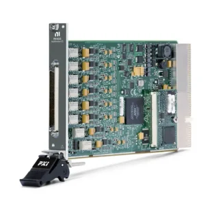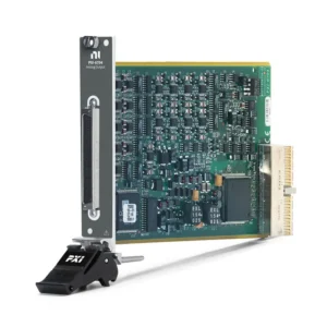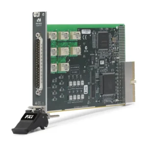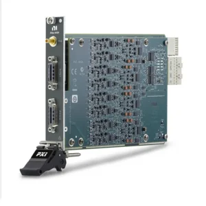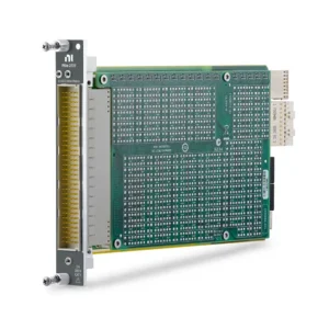


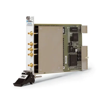
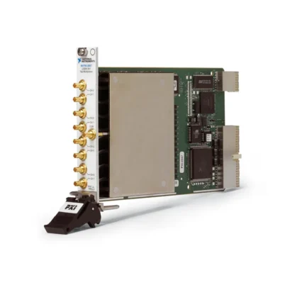
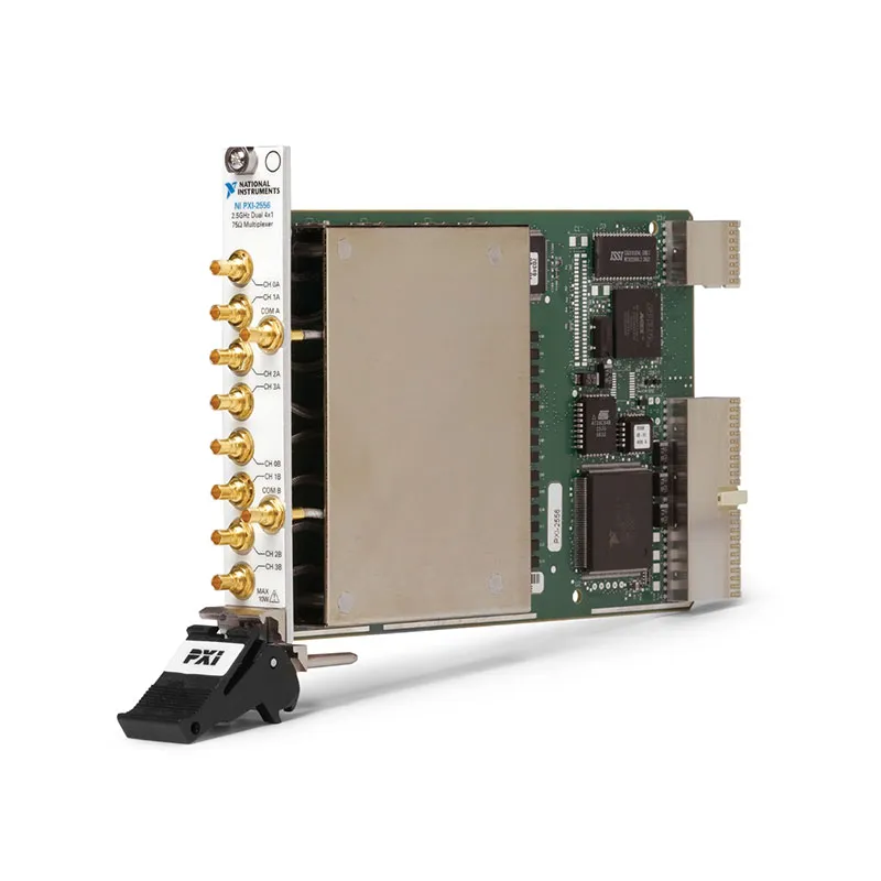
PXI-2556 2.5 GHz 75 Ω Dual 4×1 RF Multiplexer
The PXI-2556 is a dual-bank 4×1 PXI RF multiplexer switch module designed for routing video, broadcast and other high-frequency 75 Ω signals. It contains two independently controlled multiplexers, allowing two RF signal paths to operate simultaneously.
The multibank architecture is particularly useful for stimulus-and-response testing of video RF devices such as tuners, receivers, modulators and set-top boxes. One multiplexer bank can route a source to the device under test while the second bank routes the device response to an analyzer.
With DC to 2.5 GHz signal coverage, low insertion loss, controlled VSWR and onboard relay-count tracking, the PXI-2556 supports repeatable RF routing in automated production, validation and laboratory test systems.
Key Features of the PXI-2556
- Two independent 4×1 RF multiplexer banks
- Eight RF channels and two common connections
- DC to 2.5 GHz frequency coverage
- 75 Ω nominal characteristic impedance
- Unterminated RF multiplexer architecture
- 30 V maximum switching voltage
- 0.5 A maximum switching or carry current per channel
- 10 W maximum channel-to-common RF power
- Less than 1.7 dB insertion loss through 2.5 GHz
- Less than 1.75 VSWR through 2.5 GHz
- Greater than 40 dB typical isolation through 2.5 GHz
- Less than -50 dB typical bank-to-bank crosstalk at 2.5 GHz
- Less than 25 ps typical channel-to-channel skew
- Electromechanical latching relays
- Onboard relay-count tracking
- PXI hardware trigger support
- Ten gold-plated mini-75 Ω SMB connectors
- NI-SWITCH and NI Switch Executive compatibility
PXI-2556 Technical Specifications
| Product Model | PXI-2556 |
|---|---|
| Part Number | 778572-56 |
| Product Type | PXI RF multiplexer switch module |
| Topology | Dual 4×1 multiplexers, dual SP4T |
| Number of Banks | 2 independent banks |
| Channels per Bank | 4 |
| Total RF Connections | 8 channels plus 2 common ports |
| Frequency Range | DC to 2.5 GHz |
| Characteristic Impedance | 75 Ω nominal |
| Internal Termination | No; unterminated signal paths |
| Maximum Switching Voltage | 30 V |
| Maximum Switching Current | 0.5 A per channel |
| Maximum Carry Current | 0.5 A per channel |
| Maximum RF Power | 10 W channel-to-common |
| Initial DC Path Resistance | Less than 0.35 Ω typical |
| End-of-Life Path Resistance | 1.0 Ω or greater typical |
| Insertion Loss to 1 GHz | Less than 0.8 dB; less than 0.5 dB typical |
| Insertion Loss to 2 GHz | Less than 1.3 dB; less than 0.9 dB typical |
| Insertion Loss to 2.5 GHz | Less than 1.7 dB; less than 1.2 dB typical |
| VSWR to 1 GHz | Less than 1.25; less than 1.1 typical |
| VSWR to 2 GHz | Less than 1.5; less than 1.3 typical |
| VSWR to 2.5 GHz | Less than 1.75; less than 1.5 typical |
| Typical Isolation to 1 GHz | Greater than 47 dB |
| Typical Isolation to 2 GHz | Greater than 40 dB |
| Typical Isolation to 2.5 GHz | Greater than 40 dB |
| Bank-to-Bank Crosstalk to 1 GHz | Less than -58 dB typical |
| Bank-to-Bank Crosstalk to 2 GHz | Less than -53 dB typical |
| Bank-to-Bank Crosstalk to 2.5 GHz | Less than -50 dB typical |
| Channel-to-Channel Skew | Less than 25 ps typical |
| Propagation Delay | 1.0 ns typical |
| Rise Time | 75 ps typical, 10% to 90% |
| Relay Type | Electromechanical, latching |
| Maximum Relay Operate Time | 10.4 ms |
| Maximum Scan Rate | Approximately 45 channels/s |
| Mechanical Relay Life | 1 × 10⁶ cycles |
| Electrical Relay Life | 3 × 10⁵ cycles at 30 V and 10 mA resistive |
| Input Trigger Sources | PXI trigger lines 0 through 7 |
| Minimum Input Trigger Pulse Width | 150 ns with digital filtering enabled |
| Output Trigger Destinations | PXI trigger lines 0 through 7 |
| Output Trigger Pulse Width | Programmable from 1 µs to 62 µs |
| Front-Panel Connectors | 10 gold-plated mini-75 Ω SMB jacks |
| PXI Power Requirement | 3.7 W at 5 V and 0.3 W at 3.3 V |
| Software Support | NI-SWITCH and NI Switch Executive |
| Bus Interface | PXI |
| Module Format | 3U, single-slot PXI/cPCI module |
| Dimensions | 21.6 × 2.0 × 13.0 cm |
| Weight | Approximately 227 g |
| Operating Temperature | 0°C to 55°C |
| Storage Temperature | -20°C to 70°C |
| Product Status | Discontinued by NI |
PXI-2556 Part Number and Accessories
| Item | Part Number | Description |
|---|---|---|
| PXI-2556 | 778572-56 | 2.5 GHz, 75 Ω, dual 4×1 PXI RF multiplexer switch module |
| Mini-75 Ω SMB Cable | 197211-0R3 | 0.3 m mini-75 Ω SMB plug-to-plug coaxial cable |
| Mini-75 Ω SMB Cable | 197211-01 | 1 m mini-75 Ω SMB plug-to-plug coaxial cable |
| Type F to Mini-75 Ω SMB Cable | 197210-0R3 | 0.3 m Type F female to mini-75 Ω SMB plug coaxial cable |
The PXI-2556 uses ten specialized mini-75 Ω SMB connectors. Standard 50 Ω SMB and SMA cables are not direct substitutes. Verify the impedance, connector geometry, cable length and destination interface before ordering.
Dual 4×1 Multiplexer Architecture
The PXI-2556 contains two independent multiplexer banks identified as Bank A and Bank B. Each bank provides four selectable channels and one common connection.
Bank A contains CH0A through CH3A and COM A. Bank B contains CH0B through CH3B and COM B. The selected channel in each bank connects to its corresponding common port.
The two banks can operate independently, allowing the module to maintain two different RF routes at the same time.
Parallel Stimulus-and-Response Testing
The dual-bank design is useful when a device must receive an RF stimulus while its output is measured simultaneously. One bank can route a generator to the DUT input, while the second bank routes the DUT output to an analyzer.
This configuration is particularly useful for testing video tuners, receivers, modulators, set-top boxes and other RF devices with distinct input and output signal paths.
Bidirectional RF Routing
Each multiplexer bank can be used in either direction. One source connected to a common port can be routed to one of four channels, or four sources connected to the channels can be selected individually for a common analyzer.
Before connecting routes, verify that the configuration will not electrically connect incompatible sources or loads.
Unterminated Signal Paths
The PXI-2556 does not contain internal 75 Ω terminations for disconnected channels. Unselected paths remain open unless external termination is installed.
This provides lower insertion loss and avoids internal termination power limits. However, open ports can produce reflections that affect certain sources and high-frequency measurements.
Use appropriate external 75 Ω terminations when inactive channels must maintain a defined impedance.
75 Ω Characteristic Impedance
The PXI-2556 is designed for 75 Ω video and RF systems. This impedance is commonly used in broadcast, cable television, video distribution and related coaxial applications.
Use 75 Ω sources, loads, cables and adapters to maintain the specified insertion loss and VSWR. Mixing 50 Ω and 75 Ω components can create reflections and amplitude errors.
DC to 2.5 GHz Bandwidth
The module routes signals from DC through 2.5 GHz. It can handle baseband video, high-frequency video, broadcast RF, cable-device signals and other applications requiring 75 Ω signal paths.
System bandwidth depends on the complete route. Cable length, adapters, fixture layout and connected equipment can reduce overall performance.
Low Insertion Loss
Insertion loss is specified below 0.8 dB through 1 GHz, below 1.3 dB through 2 GHz and below 1.7 dB through 2.5 GHz.
Typical loss is below 0.5 dB at 1 GHz, below 0.9 dB at 2 GHz and below 1.2 dB at 2.5 GHz. This helps preserve signal amplitude in video and RF measurements.
For precision measurements, characterize each switch path together with its cables and fixture, then apply frequency-dependent loss correction.
VSWR Performance
VSWR is specified below 1.25 through 1 GHz, below 1.5 through 2 GHz and below 1.75 through 2.5 GHz.
Maintaining this performance requires correctly rated 75 Ω cables and equipment. Damaged connectors, impedance-mismatched adapters and unterminated external lines can increase reflections.
Channel Isolation
Typical isolation is greater than 47 dB through 1 GHz and greater than 40 dB through 2.5 GHz.
Isolation reduces leakage from inactive channels into a selected path. Strong RF signals can still couple through external cables or fixtures, so cable layout and shielding remain important.
Bank-to-Bank Crosstalk
Typical bank-to-bank crosstalk is below -58 dB through 1 GHz, below -53 dB through 2 GHz and below -50 dB through 2.5 GHz.
This helps Bank A and Bank B operate simultaneously with limited interaction. For sensitive measurements, keep high-power and low-level external cables separated.
Propagation Delay and Skew
Typical propagation delay through a selected path is approximately 1 ns. Typical channel-to-channel skew is less than 25 ps, and typical 10% to 90% rise time is 75 ps.
Use matched cable lengths when comparing signal timing or phase between different switch routes.
30 V, 0.5 A and 10 W Ratings
The PXI-2556 supports switching voltages up to 30 V and switching or carry current up to 0.5 A per channel. Maximum RF power is 10 W for each channel-to-common path.
The signal must remain within all voltage, current and power limits simultaneously. Peak or pulsed waveforms should be evaluated using their maximum instantaneous conditions.
Avoid Switching Active RF Signals
NI recommends against switching active RF signals whenever possible. As an electromechanical relay changes state, its path becomes momentarily unterminated, which can reflect power toward the signal source.
Reduce or disable the source before changing channels, then restore the output after relay settling. Cold switching can also improve relay life and measurement repeatability.
Latching Electromechanical Relays
The PXI-2556 uses electromechanical latching relays. A latching relay maintains its commanded state without continuously energizing its coil, helping reduce steady-state module power.
Electromechanical contacts provide low resistance and low RF loss, but they have a finite service life. Switching high-power or reactive signals can accelerate contact wear.
Relay Life and Relay-Count Tracking
Expected mechanical relay life is approximately 1 × 10⁶ cycles. Expected electrical life is approximately 3 × 10⁵ cycles at 30 V and 10 mA with a resistive load.
Onboard relay-count tracking records the activity of each signal path. Maintenance teams can identify heavily used channels and plan replacement before contact wear causes intermittent signal loss.
Hardware-Triggered Scanning
The PXI-2556 accepts triggers and exports trigger signals through PXI trigger lines 0 through 7. Hardware triggering enables deterministic coordination with RF generators, digitizers and analyzers.
The minimum input trigger pulse width is 150 ns with digital filtering enabled. Output trigger pulse width is programmable from 1 µs to 62 µs.
NI-SWITCH Software Support
The PXI-2556 is controlled using the NI-SWITCH instrument driver. NI-SWITCH provides functions for initializing the module, connecting channels, disconnecting routes, creating scan lists, configuring triggers and reading relay counts.
The driver supports LabVIEW, LabWindows/CVI and compatible text-based programming environments.
NI Switch Executive Integration
NI Switch Executive allows engineers to create meaningful route names for sources, DUT connections and analyzer inputs. This reduces the need to manage physical channel identifiers directly in application code.
Named routes can also coordinate the PXI-2556 with additional RF switch modules in larger test systems.
Typical PXI-2556 Applications
- Parallel video tuner testing
- Stimulus-and-response RF testing
- Broadcast equipment validation
- Cable television device testing
- Set-top box functional testing
- Video receiver testing
- RF generator output routing
- Analyzer input selection
- Automated production test equipment
- 75 Ω component characterization
- Modulator and demodulator testing
- Video signal distribution
- Coaxial device testing
- Laboratory RF automation
Video Tuner Testing
Bank A can route one of several RF stimulus signals to a tuner input while Bank B routes one of several tuner outputs to a measurement instrument.
This architecture enables stimulus-and-response measurements without requiring two separate switch modules.
Parallel DUT Testing
The two independent banks can also serve separate devices or fixture sections. For example, Bank A can select one DUT while Bank B selects a second signal or measurement path.
Parallel operation must remain within the module’s electrical ratings and bank-to-bank crosstalk requirements.
Automated Production Testing
The PXI-2556 replaces manual coaxial reconnection with software-controlled routes. Test sequences can select sources, DUTs and analyzers automatically.
Relay-count tracking helps production engineers plan maintenance and reduce unexpected downtime caused by worn switch contacts.
PXI-2556 Troubleshooting
The PXI-2556 Is Not Detected in NI MAX
Confirm that the module is fully installed in a compatible PXI or hybrid slot. Check chassis power, controller communication and NI-SWITCH installation, then restart the system.
No Signal Reaches the Common Port
Verify the selected bank and channel. Check the mini-75 Ω SMB cables, source output, analyzer input and NI-SWITCH route configuration.
One Multiplexer Bank Works but the Other Does Not
Confirm that the application uses the correct A or B channel names and corresponding common port. Inspect the cables on the affected bank and compare its relay counts with the working bank.
The Signal Level Is Lower Than Expected
Account for module insertion loss, cable attenuation and fixture loss. Characterize each complete route when accurate amplitude correction is required.
The Signal Has Excessive Reflections
Verify that every external component uses 75 Ω impedance. Add external termination to unused ports when required and replace damaged or mismatched cables.
A Signal in Bank A Appears in Bank B
Check external cable coupling, common grounding and fixture layout. Keep high-power and sensitive cables separated and verify that the observed leakage is consistent with the system isolation requirements.
The RF Source Shuts Down During Switching
The source may be detecting reflected power while the relay path is temporarily unterminated. Disable or reduce the source before switching.
A Channel Has Excessive Resistance
Inspect the external cable and connector, then compare the channel with another route. Increasing resistance may indicate relay-contact wear.
The Hardware Trigger Does Not Advance the Scan
Verify the selected PXI trigger line, direction, pulse width and scan-list configuration. Ensure that the scan has started before the first trigger arrives.
PXI-2556 Comparison with Similar 75 Ω RF Switches
| Model | Primary Configuration | Best Suited For |
|---|---|---|
| PXI-2554 | 2.5 GHz, 75 Ω, single 4×1 multiplexer | One unterminated four-channel RF route |
| PXI-2555 | 2.5 GHz, 75 Ω, terminated 4×1 multiplexer | Maintaining 75 Ω loading on inactive channels |
| PXI-2556 | 2.5 GHz, 75 Ω, dual 4×1 multiplexer | Parallel stimulus-and-response signal routing |
| PXI-2557 | 2.5 GHz, 75 Ω, single 8×1 multiplexer | Higher-channel-count selection to one common port |
| PXI-2558 | 2.5 GHz, 75 Ω, quad SPDT RF relay | Custom RF changeover and routing networks |
| PXI-2559 | 75 Ω RF relay architecture | Independent general-purpose video RF switching |
PXI-2556 vs PXI-2554
The PXI-2554 contains one 4×1 multiplexer, while the PXI-2556 contains two independent 4×1 banks. Both are unterminated 75 Ω modules with similar RF path specifications.
Select the PXI-2554 when only one route is required. Choose the PXI-2556 when two signals must be switched simultaneously or when stimulus and response paths must be controlled independently.
PXI-2556 vs PXI-2555
The PXI-2555 contains one internally terminated 4×1 bank. The PXI-2556 contains two unterminated 4×1 banks.
Select the PXI-2555 when inactive channels must remain connected to 75 Ω loads. Choose the PXI-2556 when two independent paths and lower insertion loss are more important.
PXI-2556 vs PXI-2557
The PXI-2556 divides eight channels into two independent 4×1 banks. The PXI-2557 combines eight channels into one 8×1 multiplexer.
Choose the PXI-2556 for two simultaneous four-channel routes. Select the PXI-2557 when one source or analyzer must select between as many as eight channels.
Recommended Related Products
- PXI-2554 4×1 RF Multiplexer
- PXI-2555 Terminated 4×1 RF Multiplexer
- PXI-2557 8×1 RF Multiplexer
- PXI-2558 Quad SPDT RF Relay Module
- PXI-2559 75 Ω RF Relay Module
- View More NI PXI and PXI Express Modules
Selecting the Right 75 Ω RF Multiplexer
Choose the PXI-2556 when the test system requires two independent 4×1 RF paths, operation through 2.5 GHz and 75 Ω signal compatibility.
Select the PXI-2554 for one four-channel path, the PXI-2555 for terminated operation or the PXI-2557 when eight channels must share one common instrument connection.
Why Choose the PXI-2556?
- Provides two independent 4×1 multiplexers
- Supports simultaneous stimulus-and-response routing
- Routes signals from DC through 2.5 GHz
- Maintains 75 Ω video and RF signal paths
- Provides low insertion loss
- Handles up to 30 V, 0.5 A and 10 W
- Offers controlled VSWR and bank isolation
- Includes onboard relay-count tracking
- Supports deterministic hardware triggering
- Integrates with NI-SWITCH and NI Switch Executive
Frequently Asked Questions
What is the PXI-2556?
The PXI-2556 is a 2.5 GHz, 75 Ω PXI RF switch module containing two independent 4×1 multiplexers.
What is the PXI-2556 part number?
The standard NI part number is 778572-56.
How many RF channels does it provide?
The module provides eight channels divided between two banks, with four channels and one common port in each bank.
What is the frequency range?
The PXI-2556 routes signals from DC through 2.5 GHz.
Are the disconnected channels internally terminated?
No. The PXI-2556 has an unterminated topology. External 75 Ω termination may be added when required.
Can both multiplexer banks operate simultaneously?
Yes. Bank A and Bank B are independently controlled and can maintain separate signal routes at the same time.
What is the maximum RF power?
Maximum channel-to-common RF power is 10 W, subject to the 30 V and 0.5 A limits.
What is the maximum insertion loss?
Insertion loss is less than 0.8 dB through 1 GHz, less than 1.3 dB through 2 GHz and less than 1.7 dB through 2.5 GHz.
What type of connectors does it use?
The front panel provides ten gold-plated mini-75 Ω SMB connectors.
Does it support relay-count tracking?
Yes. Onboard relay-count tracking helps monitor usage and schedule preventive maintenance.
Which software controls the PXI-2556?
The module is controlled using NI-SWITCH and can be integrated into named-route applications with NI Switch Executive.
Is the PXI-2556 still available from NI?
No. NI identifies the PXI-2556 as no longer available. Used, refurbished and new-surplus modules may remain available through specialized suppliers.
Request a Quote for the PXI-2556
Contact us for current availability, condition, testing options and project pricing for the PXI-2556 2.5 GHz 75 Ω Dual 4×1 RF Multiplexer. We can also help identify compatible mini-75 Ω SMB cables, PXI chassis and related PXI-2554, PXI-2555 or PXI-2557 modules.