






PXIe-7966R Virtex-5 SX95T FlexRIO FPGA Module
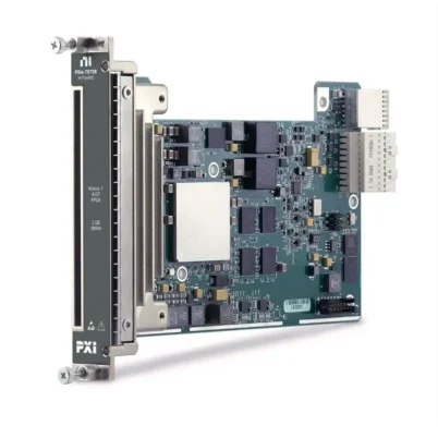
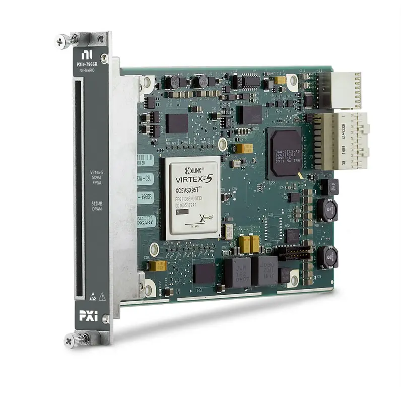
The PXIe-7966R, commonly listed as the PXIe-7966, is a PXI Express FlexRIO FPGA module designed for custom high-speed data acquisition, inline signal processing, protocol implementation and real-time test applications. It combines a user-programmable Xilinx Virtex-5 SX95T-2 FPGA with 512 MB of onboard DRAM and a high-speed interface for compatible FlexRIO adapter modules.
The PXIe-7966R does not provide fixed analog or digital measurement channels by itself. Its external I/O capabilities are determined by the installed FlexRIO adapter module. This modular architecture allows the same FPGA carrier to support digitizers, waveform generation, high-speed digital I/O, camera interfaces, RF conversion and other application-specific I/O.
Key Features of the PXIe-7966R
- Xilinx Virtex-5 SX95T-2 user-programmable FPGA
- 14,720 FPGA slices
- 58,880 lookup tables and flip-flops
- 640 DSP48 arithmetic slices
- 8,784 kbits of embedded block RAM
- 512 MB onboard DRAM
- Two independent 256 MB DRAM banks
- Up to 1.6 GB/s bandwidth per DRAM bank
- 66 differential LVDS pairs for adapter-module communication
- PXI Express system interface
- More than 800 MB/s streaming into or out of the module
- More than 1.4 GB/s aggregate bidirectional streaming
- Up to 16 DMA data streams
- Peer-to-peer data streaming support
- PXIe_CLK100 reference-clock support
- Programmable with the LabVIEW FPGA Module
PXIe-7966R Technical Specifications
| Product Model | PXIe-7966R / PXIe-7966 |
|---|---|
| Part Number | 781805-01 |
| Product Type | PXI Express FlexRIO FPGA module |
| FPGA | Xilinx Virtex-5 SX95T-2 |
| FPGA Speed Grade | -2 |
| FPGA Slices | 14,720 |
| Lookup Tables and Flip-Flops | 58,880 |
| DSP48 Slices | 640 |
| DSP Multiplier Size | 25 × 18 bits |
| Embedded Block RAM | 8,784 kbits |
| Onboard DRAM | 512 MB total |
| DRAM Configuration | Two banks, 256 MB per bank |
| DRAM Bandwidth | Up to 1.6 GB/s per bank |
| Adapter Interface | 66 differential LVDS pairs |
| Default FPGA Timebase | 40 MHz |
| Reference Clock Source | PXI Express 100 MHz reference clock, PXIe_CLK100 |
| Module Streaming Rate | More than 800 MB/s into or out of the module |
| Simultaneous Bidirectional Streaming | More than 700 MB/s per direction |
| Aggregate Bidirectional Rate | More than 1.4 GB/s |
| Maximum DMA Streams | Up to 16 |
| Peer-to-Peer Streaming | Supported |
| Bus Interface | PXI Express |
| Programming Environment | LabVIEW FPGA Module |
| Device Driver | NI FlexRIO |
| Module Format | 3U PXI Express module |
| Product Status | Discontinued |
| Recommended Successor | PXIe-7976R for compatible migration projects |
PXIe-7966R Part Number and Identification
| Identifier Type | Number | Description |
|---|---|---|
| Orderable Part Number | 781805-01 | PXIe-7966R FlexRIO FPGA module with Virtex-5 SX95T and 512 MB RAM |
| Assembly Number | 198733-04L | PXIe-7966R circuit-card assembly with 66 LVDS pairs and SX95T-2 FPGA |
The assembly number printed on the internal circuit card is not normally used as the commercial ordering number. Use 781805-01 when identifying the complete PXIe-7966R module for a quotation or replacement.
FlexRIO Modular Architecture
FlexRIO separates the FPGA processing resource from the application-specific I/O. The PXIe-7966R provides the FPGA, onboard memory, PXI Express communication and timing resources, while a compatible adapter module provides the required analog, digital, RF or camera interface.
This architecture allows engineers to select an adapter according to the signal requirements and develop FPGA logic specifically for the application. However, the FPGA carrier and adapter must be electrically, mechanically and software compatible.
Virtex-5 SX95T-2 FPGA
The PXIe-7966R uses a Xilinx Virtex-5 SX95T FPGA with a -2 speed grade. This differentiates it from the PXIe-7965R, which uses the same basic SX95T architecture with a slower speed grade.
The FPGA executes application logic directly in hardware, providing deterministic timing and parallel processing without depending on the operating-system scheduling of the PXI controller.
14,720 FPGA Slices
The Virtex-5 SX95T provides 14,720 FPGA slices for implementing control logic, state machines, data routing, protocol processing and application-specific algorithms.
NI documentation may also express device capacity as 58,880 lookup tables and flip-flops. Resource usage depends on the LabVIEW FPGA design, clock rates, data types, memory implementation and compilation optimization.
640 DSP48 Slices
The PXIe-7966R includes 640 DSP48 slices designed for hardware-accelerated mathematical processing. These resources can implement multipliers, filters, mixers, decimation, interpolation and other signal-processing operations.
The high DSP resource count makes the module suitable for applications involving digital filtering, frequency conversion, image processing and real-time spectral algorithms.
Embedded FPGA Block RAM
The FPGA provides 8,784 kbits of embedded block RAM. Block RAM offers low-latency storage directly inside the FPGA fabric and can be used for FIFOs, lookup tables, delay lines, buffering and algorithm state.
Block RAM is faster and more deterministic than external DRAM, but its capacity is much smaller. FPGA applications commonly use block RAM for immediate processing and onboard DRAM for larger data buffers.
512 MB Onboard DRAM
The PXIe-7966R includes 512 MB of onboard DRAM organized as two independent 256 MB banks. Each bank supports bandwidth up to approximately 1.6 GB/s under supported access conditions.
Onboard DRAM can buffer high-speed acquisitions, hold generated waveforms or store intermediate processing results before data is transferred to the controller or another PXI Express instrument.
Using the Two DRAM Banks
The two-bank architecture allows an FPGA design to distribute memory traffic across independent resources. For example, one bank can receive acquired data while the second stores processed results or generation data.
Efficient DRAM use requires correctly structured request and retrieval logic. Poor access patterns or insufficient buffering can reduce achievable throughput even when the theoretical memory bandwidth is high.
66-Pair LVDS Adapter Interface
The PXIe-7966R provides 66 differential LVDS pairs between the FPGA carrier and an installed FlexRIO adapter module. These lines support high-speed, low-voltage communication between application-specific I/O circuitry and the FPGA.
The LVDS pairs are part of the internal FlexRIO adapter interface and should not be treated as general front-panel I/O without a compatible adapter module. Actual channel count, direction and electrical characteristics depend on the adapter.
Compatible FlexRIO Adapter Modules
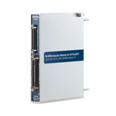
The PXIe-7966R can operate with compatible first-generation FlexRIO adapter modules for analog input, analog output, digital I/O, RF conversion and image acquisition. Examples from the FlexRIO ecosystem include high-speed digitizer and signal-generation adapter modules.
Compatibility should be verified using the specific adapter documentation and supported NI FlexRIO software version. Newer integrated-I/O or Kintex-based FlexRIO devices may use a different architecture and should not be assumed to accept the same adapter.
Adapter Module Determines the I/O
The PXIe-7966R alone does not specify sample rate, analog resolution, input voltage, output voltage or digital logic level. These specifications come from the installed adapter module.
When ordering a FlexRIO system, identify both the FPGA carrier and the required adapter. A PXIe-7966R without an adapter cannot directly connect to the external measurement signal.
High-Speed PXI Express Streaming
The PXIe-7966R can stream data at more than 800 MB/s into or out of the module when the chassis and controller configuration provide sufficient bandwidth.
When streaming simultaneously in both directions, supported configurations can exceed 700 MB/s per direction, providing an aggregate rate above 1.4 GB/s. Actual throughput depends on the FPGA design, DMA configuration, chassis topology and controller performance.
Up to 16 DMA Streams
The module supports as many as 16 DMA channels. Multiple DMA streams can separate acquired data, processed results, control information and waveform-generation data.
The number of enabled streams and bandwidth assigned to each stream are determined by the FPGA design. Using more streams does not increase the physical PXI Express bandwidth, so the total data rate must remain within system limits.
Peer-to-Peer Streaming
NI peer-to-peer streaming allows the PXIe-7966R to exchange data directly with compatible PXI Express instruments without routing every transfer through the controller CPU and host memory.
For example, a compatible digitizer can stream acquired samples directly to the PXIe-7966R for FPGA processing. The processed data can then be sent to another FPGA module, generator or supported instrument.
Benefits of Peer-to-Peer Processing
Peer-to-peer transfer can reduce controller workload and data-transfer latency. It is useful for closed-loop testing, real-time spectral processing, high-speed triggering and applications where the raw data rate would place a significant load on the host system.
Peer-to-peer compatibility depends on the instruments, PXI Express chassis topology, slot selection, driver versions and FPGA endpoint configuration.
PXI Express Timing and Synchronization
The PXIe-7966R uses the PXIe_CLK100 reference clock as a timing source and provides a default FPGA timebase of 40 MHz. FPGA-derived clocks can be used to implement application-specific timing domains.
PXI trigger resources allow the FPGA application to coordinate acquisition, generation and processing with other instruments in the chassis. Timing behavior ultimately depends on the FPGA bitfile and adapter-module implementation.
Deterministic FPGA Processing
Algorithms implemented in the FPGA operate in hardware with defined clock-cycle timing. This supports deterministic triggering, custom protocols and low-latency control that would be difficult to achieve using only software running on the PXI controller.
Parallel FPGA logic can perform multiple operations at the same time, including data capture, filtering, decision-making and transfer to memory or another instrument.
LabVIEW FPGA Programming
The PXIe-7966R is programmed with the LabVIEW FPGA Module and supported NI FlexRIO software. Developers create FPGA logic graphically, compile the design into a bitfile and download the bitfile to the module.
Compilation targets the Virtex-5 SX95T-2 device and can require a compatible Xilinx compilation toolchain. Verify operating-system, LabVIEW, LabVIEW FPGA and FlexRIO driver compatibility before rebuilding an older project.
Using Existing FPGA Bitfiles
An existing deployment may run a previously compiled FPGA bitfile without recompiling the original project, provided the application, driver and hardware remain compatible.
Recompilation may be necessary when changing the FPGA logic, adapter module, LabVIEW version or target hardware. Preserve the source project, compilation settings and validated bitfiles when maintaining legacy systems.
Typical PXIe-7966R Applications
- High-speed data acquisition
- Inline digital signal processing
- Custom protocol implementation
- Radar and communications testing
- Software-defined radio processing
- Machine vision and camera interfacing
- High-speed digital I/O
- Custom triggering and event detection
- Hardware-in-the-loop testing
- Real-time spectrum processing
- Peer-to-peer instrument streaming
- Research and laboratory automation
High-Speed Data Acquisition
When combined with a compatible digitizer adapter, the PXIe-7966R can acquire high-speed analog signals and process them directly in the FPGA. Data can be filtered, decimated, triggered or reduced before transfer to the host controller.
FPGA preprocessing can significantly reduce host data volume when the application only needs detected events, calculated parameters or selected waveform segments.
Real-Time Signal Processing
The 640 DSP48 slices support parallel filtering, mixing and mathematical processing. Algorithms can operate continuously on incoming samples with deterministic hardware timing.
Applications include digital downconversion, channelization, pulse detection, modulation processing and real-time frequency-domain analysis.
Custom Digital Protocols
A compatible digital adapter module allows the PXIe-7966R to implement nonstandard or application-specific communication protocols. FPGA logic can control exact edge timing, framing, encoding and response behavior.
This capability is useful when validating proprietary devices or legacy interfaces not supported by conventional digital instruments.
Hardware-in-the-Loop Testing
The module can implement deterministic models, signal processing and custom I/O behavior for hardware-in-the-loop systems. Peer-to-peer streaming can connect the FPGA directly with supported digitizers, generators and other modules.
System latency depends on the adapter, FPGA code, memory use, peer-to-peer path and the timing requirements of the complete test system.
Machine Vision Applications
With an appropriate camera adapter, the PXIe-7966R can receive and process image data in real time. FPGA logic can perform pixel-level operations, region detection, thresholding and data reduction before frames reach the controller.
Verify camera standard, adapter compatibility, pixel clock and required data throughput before selecting the complete system.
PXIe-7966R Troubleshooting
The PXIe-7966R Is Not Detected in NI MAX
Confirm that the module is fully installed in a compatible PXI Express slot. Check chassis power, controller communication, NI FlexRIO installation and driver compatibility, then rescan the system in NI Measurement & Automation Explorer.
The Adapter Module Is Not Recognized
Verify that the adapter is correctly seated and compatible with the PXIe-7966R. Check the adapter documentation and installed FlexRIO support version.
The FPGA Bitfile Will Not Download
Confirm that the bitfile was compiled for the PXIe-7966R and the installed adapter configuration. A bitfile compiled for a different FPGA target cannot normally be loaded onto this module.
The FPGA Project Does Not Compile
Check the LabVIEW FPGA version, FlexRIO driver and required Xilinx compilation tools. Older Virtex-5 targets may require a legacy software environment that is not included with current LabVIEW releases.
DMA Throughput Is Lower Than Expected
Review DMA buffer sizes, host memory allocation, controller performance, chassis topology and FPGA loop timing. Confirm that the selected PXI Express slot provides the required data path.
Onboard DRAM Produces Timing Errors
Check the request and retrieval sequence, memory address range and buffering logic. Use the correct DRAM interface methods and monitor error terminals for invalid or out-of-range memory access.
Peer-to-Peer Streaming Does Not Start
Confirm that both endpoints support NI peer-to-peer streaming and that the chassis topology provides a valid route. Verify endpoint configuration, writer and reader compatibility, data type and FIFO setup.
FPGA Resource Utilization Is Too High
Review lookup-table, flip-flop, DSP and block-RAM use in the compilation report. Reduce parallel logic, reuse arithmetic resources or move large buffers from block RAM to onboard DRAM when the application permits.
The Application Runs on the PXIe-7965R but Not the PXIe-7966R
The modules use similar FPGA architectures but are separate compilation targets with different FPGA speed grades. Recompile and validate the project for the exact target module.
The Module Overheats or Becomes Unstable
Verify chassis airflow, fan configuration and adjacent-module cooling. High FPGA utilization and continuous high-speed I/O can increase thermal load.
PXIe-7966R Comparison with Similar FlexRIO FPGA Modules
| Model | FPGA and Memory | Best Suited For |
|---|---|---|
| PXIe-7962R | Virtex-5 SX50T, 512 MB DRAM | Legacy applications requiring fewer FPGA processing resources |
| PXIe-7965R | Virtex-5 SX95T, 512 MB DRAM | Existing SX95T projects that do not require the faster -2 speed grade |
| PXIe-7966R | Virtex-5 SX95T-2, 512 MB DRAM | Highest-performance target in the PXIe-796x FlexRIO family |
| PXIe-7972R | Kintex-7 K325T, 2 GB DRAM | Newer projects needing additional FPGA and memory resources |
| PXIe-7976R | Kintex-7 K410T, 2 GB DRAM | Migration from legacy FlexRIO modules and demanding FPGA applications |
PXIe-7966R vs PXIe-7965R
The PXIe-7966R and PXIe-7965R both use a Virtex-5 SX95T FPGA, provide 640 DSP48 slices and include 512 MB of DRAM. The PXIe-7966R uses a faster -2 FPGA speed grade.
Choose the PXIe-7966R when the validated application specifically requires this target or benefits from its faster speed grade. Existing PXIe-7965R bitfiles should not be assumed to work without recompilation and validation.
PXIe-7966R vs PXIe-7962R
The PXIe-7962R uses a smaller Virtex-5 SX50T FPGA with 288 DSP slices and 4,752 kbits of block RAM. The PXIe-7966R provides substantially more DSP and embedded-memory resources.
Select the PXIe-7966R for larger signal-processing algorithms and greater FPGA capacity. The PXIe-7962R may be sufficient for less complex legacy applications.
PXIe-7966R vs PXIe-7976R
The PXIe-7976R uses a newer Kintex-7 K410T FPGA, includes 2 GB of DRAM and provides significantly higher FPGA and data-transfer performance than the PXIe-7966R.
NI identified the PXIe-7976R as the migration option for discontinued PXIe-7966R applications. Migration can require FPGA-code changes, recompilation, performance validation and confirmation of adapter compatibility.
Recommended Related Products
- PXIe-7965R Virtex-5 SX95T FlexRIO FPGA Module
- PXIe-7962R Virtex-5 SX50T FlexRIO FPGA Module
- PXIe-7972R Kintex-7 FlexRIO FPGA Module
- PXIe-7975R Kintex-7 FlexRIO FPGA Module
- PXIe-7976R Kintex-7 K410T FlexRIO FPGA Module
- View More NI PXI and PXI Express Modules
Selecting the Right FlexRIO FPGA Module
Choose the PXIe-7966R when maintaining an existing FlexRIO system developed for the Virtex-5 SX95T-2 target, particularly when validated FPGA code and adapter hardware are already available.
For a new system, consider the PXIe-7976R or a current FlexRIO integrated-I/O platform. Newer modules provide more FPGA resources, additional DRAM and higher data-transfer performance but may require a redesigned software and hardware architecture.
Purchasing a Discontinued PXIe-7966R
NI changed the PXIe-7966R to discontinued status, with the final purchase period ending in 2024. Available units may therefore be unused surplus, previously installed or refurbished equipment.
Before ordering, verify the complete part number, serial number, adapter compatibility and physical condition. A used module should be tested for PXI enumeration, FPGA bitfile download, DRAM access, DMA transfer, peer-to-peer operation and communication with the intended adapter.
Why Choose the PXIe-7966R?
- Maintains compatibility with legacy Virtex-5 FlexRIO applications
- Provides 640 DSP48 slices for real-time signal processing
- Includes 512 MB of onboard DRAM
- Supports high-speed modular I/O through FlexRIO adapters
- Streams data at more than 800 MB/s in supported systems
- Supports as many as 16 DMA streams
- Provides peer-to-peer data transfer between compatible instruments
- Offers deterministic FPGA-based control and processing
- Integrates with LabVIEW FPGA and PXI Express systems
Frequently Asked Questions
What Is the PXIe-7966R?
The PXIe-7966R is a PXI Express FlexRIO FPGA carrier module with a user-programmable Virtex-5 SX95T-2 FPGA and 512 MB of onboard DRAM.
Are PXIe-7966 and PXIe-7966R the Same Product?
Yes. NI documentation commonly uses PXIe-7966R, while some product listings shorten the model name to PXIe-7966. The R identifies its reconfigurable FPGA architecture.
What Is the PXIe-7966R Part Number?
The standard commercial part number is 781805-01.
Which FPGA Does the PXIe-7966R Use?
The module uses a Xilinx Virtex-5 SX95T FPGA with a -2 speed grade.
How Much DRAM Does It Provide?
The PXIe-7966R provides 512 MB of onboard DRAM divided into two 256 MB banks.
Does the PXIe-7966R Include Analog Inputs?
Not by itself. Analog, digital, RF or camera I/O is provided by a compatible FlexRIO adapter module installed on the FPGA carrier.
How Many LVDS Pairs Does It Provide?
The internal interface between the FPGA module and adapter provides 66 differential LVDS pairs.
What Is the Maximum Streaming Rate?
Supported systems can exceed 800 MB/s in one direction. Simultaneous bidirectional operation can exceed 700 MB/s per direction and 1.4 GB/s aggregate.
Does It Support Peer-to-Peer Streaming?
Yes. The PXIe-7966R supports direct peer-to-peer transfer with compatible PXI Express instruments and chassis configurations.
Which Software Is Required?
Development normally requires compatible versions of the NI FlexRIO driver, LabVIEW and the LabVIEW FPGA Module. FPGA compilation may also require the appropriate legacy Xilinx tools.
Can an Existing PXIe-7966R Bitfile Run on a PXIe-7976R?
No direct compatibility should be assumed. The PXIe-7976R uses a different FPGA architecture, so the project generally requires migration, recompilation and system validation.
What Replaced the PXIe-7966R?
NI identified the PXIe-7976R as the replacement or migration option, although adapter and software compatibility must be evaluated for the individual application.
Is the PXIe-7966R Still Manufactured?
No. The PXIe-7966R is discontinued, and availability is generally limited to surplus or previously installed modules.
Request a Quote for the PXIe-7966R
Contact us for current availability, condition and project pricing for the PXIe-7966R Virtex-5 SX95T FlexRIO FPGA Module. We can also help verify the 781805-01 part number, adapter-module compatibility, software requirements and suitable PXIe-7976R migration options for your test system.















