






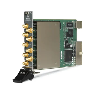
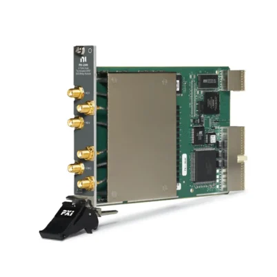

PXI-2548 2.7 GHz Quad SPDT PXI RF Relay Module
The PXI-2548 is a 2.7 GHz, 50 Ω PXI RF relay module designed for automated RF testing, signal routing and switch-network development. It provides four independent single-pole double-throw relay banks, each with normally closed, normally open and common RF connections.
The quad SPDT architecture can route four independent common signals between two possible paths. With low insertion loss, controlled VSWR, high isolation and twelve gold-plated SMA connectors, the PXI-2548 is suitable for connecting RF sources, analyzers, devices under test and other switch modules.
Key Features of the PXI-2548
- Four independent SPDT RF relay banks
- DC to 2.7 GHz switching bandwidth
- 50 Ω nominal characteristic impedance
- Normally closed, normally open and common connections for each bank
- Twelve gold-plated SMA female connectors
- 30 V maximum switching voltage
- 0.5 A maximum switching or carry current
- 10 W maximum RF switching power
- Less than 1 dB insertion loss through 2.7 GHz
- Less than 1.7 VSWR through 2.7 GHz
- Greater than 39 dB typical isolation through 2.7 GHz
- Less than -45 dB typical crosstalk through 2.7 GHz
- Less than 15 ps typical channel-to-channel skew
- 710 ps typical propagation delay
- 55 ps typical rise time
- Latching electromechanical RF relays
- Onboard relay-count tracking
- PXI hardware trigger support
- NI-SWITCH and NI Switch Executive compatibility
PXI-2548 Technical Specifications
| Product Model | PXI-2548 |
|---|---|
| Part Number | 778572-48 |
| Product Type | PXI RF relay module |
| Topology | Quad SPDT |
| Number of Relay Banks | 4 |
| Connections per Bank | Normally closed, normally open and common |
| Frequency Range | DC to 2.7 GHz |
| Characteristic Impedance | 50 Ω nominal |
| Maximum Switching Voltage | 30 V |
| Maximum Switching Current | 0.5 A per channel |
| Maximum Carry Current | 0.5 A per channel |
| Maximum RF Power | 10 W |
| Minimum Switch Load | 0 dBm |
| Initial DC Path Resistance | Less than 0.25 Ω, typical |
| End-of-Life Path Resistance | 1 Ω or greater, typical |
| Insertion Loss Through 1.5 GHz | Less than 0.7 dB; less than 0.5 dB typical |
| Insertion Loss Through 2.7 GHz | Less than 1 dB; less than 0.65 dB typical |
| VSWR Through 1.5 GHz | Less than 1.4; less than 1.25 typical |
| VSWR Through 2.7 GHz | Less than 1.7; less than 1.25 typical |
| Isolation Through 1.5 GHz | Greater than 58 dB, typical |
| Isolation Through 2.7 GHz | Greater than 39 dB, typical |
| Crosstalk Through 1.5 GHz | Less than -60 dB, typical |
| Crosstalk Through 2.7 GHz | Less than -45 dB, typical |
| Channel-to-Channel Skew | Less than 15 ps, typical |
| Propagation Delay | 710 ps, typical |
| Rise Time | 55 ps, typical |
| Maximum Relay Operate Time | 10.4 ms |
| Maximum Scan Rate | 45 channels/s |
| Mechanical Relay Life | 1 × 10⁶ cycles |
| Electrical Relay Life | 3 × 10⁵ cycles at 30 V, 10 mA resistive |
| Relay Type | Electromechanical, latching |
| Input Trigger Sources | PXI trigger lines 0 through 7 |
| Minimum Input Trigger Pulse Width | 150 ns with digital filtering enabled |
| Output Trigger Destinations | PXI trigger lines 0 through 7 |
| Output Trigger Pulse Width | Programmable from 1 µs to 62 µs |
| Front-Panel Connectors | 12 gold-plated SMA female connectors |
| Bus Connection | PXI Hybrid |
| PXI Power Requirement | 3.7 W at 5 V and 0.3 W at 3.3 V |
| Module Format | 3U, one-slot PXI/cPCI module |
| Dimensions | 21.6 cm × 2.0 cm × 13.0 cm |
| Weight | 255 g |
| Operating Temperature | 0°C to 55°C |
| Storage Temperature | -20°C to 70°C |
| Software Support | NI-SWITCH and NI Switch Executive |
PXI-2548 Part Number and Accessories
| Item | Part Number | Description |
|---|---|---|
| PXI-2548 | 778572-48 | 2.7 GHz, 50 Ω, quad SPDT PXI RF relay module |
| SMA 100 Flexible Cable | 763443-01 | 0.15 m SMA male-to-SMA male flexible RF cable |
| SMA 100 Flexible Cable | 763444-01 | 0.45 m SMA male-to-SMA male flexible RF cable |
| MCX-to-SMA Cable | 188377-0R3 | 0.3 m MCX plug-to-SMA plug RF cable |
| MCX-to-SMA Cable | 188377-01 | 1 m MCX plug-to-SMA plug RF cable |
| SMA 50 Ω Termination | 778353-01 | 50 Ω SMA termination plug for unused RF connections |
| SMA Torque Wrench | 187106-01 | Torque wrench for correctly installing SMA connectors |
| SMA-to-SMB Adapter | 779674-01 | SMA plug-to-SMB jack RF adapter |
The PXI-2548 provides twelve front-panel SMA connectors. Each of its four relay banks has one NC, one NO and one COM connection. Use 50 Ω cables, adapters and terminations throughout the RF signal path.
Quad SPDT RF Relay Architecture
The PXI-2548 contains four independent SPDT relay banks. Each bank routes its common connection to either the normally closed or normally open RF path.
Because the four banks operate independently, the module can control four separate two-way RF routes. This architecture is useful for instrument selection, bypass switching, source selection and building custom multiplexer networks.
The four banks can also be combined externally to create larger switching structures while maintaining similar signal-path lengths across multiple channels.
SPDT Form C Operation
An SPDT relay is a single-pole double-throw switch. One common connection is routed between two possible paths identified as normally closed and normally open.
In RF systems, this topology can switch one instrument between two DUTs, select one of two RF sources or insert and bypass a component in a signal path.
The NC, NO and COM connections for each bank are accessible through separate SMA connectors, providing flexibility for custom RF test-system wiring.
Four Independent RF Banks
The four relay banks do not share a common RF connection. Each bank has an independent signal path and can be controlled separately through software.
This design allows the PXI-2548 to perform four unrelated switching operations or operate all banks as part of a larger coordinated route.
Independent banks are useful when a test system requires several sources, analyzers, amplifiers, filters or DUT connections to be switched simultaneously.
DC to 2.7 GHz Frequency Coverage
The PXI-2548 routes signals from DC through 2.7 GHz. This frequency range supports RF validation, wireless testing, communications equipment and general-purpose high-frequency signal routing.
Insertion loss, VSWR, isolation and crosstalk vary with frequency. RF performance should be evaluated at the application’s highest operating frequency.
50 Ω Characteristic Impedance
The module has a nominal characteristic impedance of 50 Ω, matching most RF signal generators, spectrum analyzers, vector signal analyzers, power meters and communication test instruments.
All connected cables, adapters, fixtures and instruments should also use 50 Ω impedance. Mixing different impedances can increase reflected power and measurement uncertainty.
Nonterminated RF Paths
The PXI-2548 does not contain internal 50 Ω terminations on its switched ports. The inactive throw remains unterminated unless an external termination is installed.
External SMA termination plugs may be required when unused ports must present a controlled impedance. This is particularly important when the inactive path remains connected to a sensitive RF source or DUT.
Insertion Loss Performance
Insertion loss represents the RF power lost as the signal passes through the selected relay path. Lower insertion loss helps preserve the signal level delivered to the analyzer or device under test.
Through 1.5 GHz, insertion loss is specified below 0.7 dB, with a typical value below 0.5 dB. Through 2.7 GHz, it remains below 1 dB, with a typical value below 0.65 dB.
These values apply to the module path. Coaxial cables, adapters, connectors and other switches contribute additional loss that should be included in system calibration.
VSWR Performance
Voltage standing wave ratio indicates the impedance match of the selected RF path. Lower VSWR means less power is reflected toward the RF source.
The PXI-2548 has specified VSWR below 1.4 through 1.5 GHz and below 1.7 through 2.7 GHz. Typical VSWR is below 1.25 across both ranges.
Correct SMA connector torque, clean interfaces, suitable cables and 50 Ω terminations help maintain system-level VSWR.
RF Isolation
Isolation measures the module’s ability to prevent RF energy from coupling through an unselected relay path.
Typical isolation is greater than 58 dB through 1.5 GHz and greater than 39 dB through 2.7 GHz. High isolation reduces leakage between the NC and NO connections.
External cable placement, shielding and grounding also affect the total isolation achieved by the test system.
Bank-to-Bank Crosstalk
Crosstalk describes unwanted RF coupling between separate relay banks. Typical crosstalk is below -60 dB through 1.5 GHz and below -45 dB through 2.7 GHz.
Keep high-power RF cables separated from sensitive receiver paths and use properly shielded coaxial cables to maintain system-level crosstalk performance.
Channel-to-Channel Skew
The PXI-2548 provides typical channel-to-channel skew below 15 ps. Low skew helps maintain similar timing when signals are routed through different relay banks.
External cable-length differences may introduce more skew than the internal switch. Use equal-length or phase-matched cables when phase and timing consistency are important.
Propagation Delay and Rise Time
The typical propagation delay is 710 ps, and the typical 10% to 90% rise time is 55 ps.
Propagation delay should be included when aligning switched RF paths with other channels. Total delay also includes external cables, adapters, fixtures and connected instruments.
10 W RF Power Handling
The maximum RF switching power is 10 W. Each selected channel must also remain within the 30 V and 0.5 A electrical limits.
For modulated or pulsed signals, confirm both average and peak power. Poor impedance matching can increase voltage at the relay and may reduce the available power margin.
30 V and 0.5 A Ratings
The PXI-2548 supports a maximum switching voltage of 30 V and a maximum switching or carry current of 0.5 A per channel.
Voltage, current and RF power ratings apply simultaneously. The module should not be used when any individual limit could be exceeded.
Switching Active RF Signals
NI recommends avoiding active RF switching whenever possible. During relay operation, a channel becomes momentarily unterminated and can reflect RF power toward the signal source.
Some RF generators and amplifiers may be damaged by severe mismatch. Reduce or disable the RF output before changing routes when required by the source documentation.
Switching active RF signals below 0 dBm may also reduce relay life and degrade signal integrity.
Latching Electromechanical Relays
The PXI-2548 uses latching electromechanical RF relays. Once switched, a relay retains its position without requiring continuous coil power.
Latching operation reduces steady-state power consumption and internal heat. The application should explicitly initialize the relay routes when the PXI system starts.
Relay Operating Time and Scan Rate
Maximum relay operating time is 10.4 ms, and the maximum scan rate is 45 channels per second.
Actual test throughput also depends on RF source settling, measurement acquisition time, DUT response and any additional delay required for signal stabilization.
Relay Life and Count Tracking
The mechanical relay life is rated at up to one million operations. Expected electrical life is approximately 300,000 cycles when switching a 30 V, 10 mA resistive load.
Actual relay life depends on voltage, current, RF power, load characteristics and whether active signals are switched.
Onboard relay-count tracking helps maintenance teams monitor usage, balance routes and replace heavily used modules before contact degradation causes unexpected downtime.
PXI Hardware Triggering
The PXI-2548 supports input and output triggers through PXI trigger lines 0 through 7. Hardware triggering allows RF switching to be synchronized with signal generators, analyzers and other PXI instruments.
The minimum input-trigger pulse width is 150 ns with digital filtering enabled. Output-trigger pulse width can be programmed from 1 µs to 62 µs.
Typical PXI-2548 Applications
- Automated RF signal routing
- RF source selection
- RF analyzer input selection
- Signal-path bypass switching
- Filter and amplifier insertion
- High-channel-count multiplexer construction
- Multiple-DUT production testing
- Wireless device validation
- Receiver and transmitter testing
- Antenna-path switching
- RF component characterization
- Communications equipment testing
- Laboratory RF automation
RF Source Selection
Each SPDT bank can select between two RF sources and route the selected signal to one common output. This allows test software to change stimulus sources without manual cable changes.
Before switching, verify that the two sources cannot become electrically connected through external wiring. Disable active outputs when required to prevent reflections.
RF Analyzer Input Selection
A common analyzer input can be switched between two DUT signals. With four independent banks, the PXI-2548 can provide four separate two-way analyzer or receiver selections.
Apply path-specific insertion-loss correction when accurate power measurements are required.
Filter and Amplifier Bypass Testing
An SPDT relay can route a signal through a filter, amplifier or other RF component in one state and through a bypass path in the other state.
This configuration supports direct comparison of component performance, gain, loss and frequency response under software control.
Building Larger RF Multiplexers
The four SPDT banks can be combined to create larger custom multiplexer networks. The module is useful when the test system requires routing flexibility not provided by a fixed multiplexer topology.
Cascading relay paths increases total insertion loss and propagation delay. System design should minimize the number of relay stages in the active path.
Uniform Signal-Path Design
The PXI-2548 can help create RF networks with similar numbers of relay stages across multiple routes. Uniform paths simplify loss correction and improve consistency among channels.
External cables should also have similar length and construction when phase, delay and insertion-loss matching are important.
Wireless Production Testing
Production systems can use the module to share RF generators and analyzers between DUT positions or test fixtures. Software-controlled switching improves repeatability and instrument utilization.
Relay-count monitoring can support preventive maintenance in high-volume production environments.
NI-SWITCH Software Support
The PXI-2548 is controlled through the NI-SWITCH instrument driver. NI-SWITCH provides functions for initializing the module, selecting NC or NO routes, disconnecting paths, creating scans and configuring triggers.
The driver supports LabVIEW, LabWindows/CVI and compatible text-based programming environments. It can also be integrated with NI TestStand test sequences.
NI Switch Executive Integration
NI Switch Executive allows engineers to define meaningful route and route-group names instead of controlling each relay directly in application code.
Named routes simplify RF systems containing several switch modules, sources, analyzers and DUT interfaces. Route validation can help prevent conflicting or invalid connections.
PXI Chassis Integration
The PXI-2548 occupies one slot in a compatible PXI or PXI hybrid-slot chassis. It can operate with signal generators, analyzers, digitizers and other NI PXI modules.
Before installation, verify chassis compatibility, cooling, controller communication, SMA cable clearance and the installed NI-SWITCH version.
PXI-2548 Troubleshooting
The PXI-2548 is not detected in NI MAX
Confirm that the module is fully installed in a compatible PXI slot. Check chassis power, controller communication and NI-SWITCH installation, then restart NI Measurement & Automation Explorer.
A relay bank does not switch between NC and NO
Verify the bank name and route command used by the application. Check the corresponding NC, NO and COM cables, source outputs and external wiring.
Insertion loss is higher than expected
Inspect SMA connectors, cables and adapters for damage, contamination or incorrect torque. Confirm that every component is rated for 2.7 GHz and include external cable loss in the calculation.
VSWR is too high
Verify that the complete signal path uses 50 Ω components. Check for loose SMA connectors, damaged cables, mixed-impedance equipment and unterminated inactive ports.
Isolation is lower than expected
Review fixture shielding, cable separation and grounding. Check whether external cables are coupling signals around the relay module.
Crosstalk appears between relay banks
Separate high-power and low-level RF cables physically. Use high-quality shielded coaxial cables and verify that leakage is not occurring through connected instruments or DUT fixtures.
The RF source becomes unstable during switching
Disable or reduce RF output power before changing routes. The relay path is momentarily unterminated during operation and may create a high reflection toward the source.
Measurements differ between relay banks
Compare cable length, connector condition, insertion loss and fixture design for each bank. Apply bank-specific loss correction if required.
A relay becomes intermittent
Check the SMA connector and cable before evaluating the internal relay. Review the relay count and test path resistance to determine whether the relay requires service.
PXI-2548 Comparison with Similar RF Switch Modules
| Model | Primary Configuration | Best Suited For |
|---|---|---|
| PXI-2545 | Terminated RF multiplexer architecture | Applications requiring internally terminated inactive paths |
| PXI-2546 | Dual-bank RF multiplexer architecture | Routing two independent groups of RF signals |
| PXI-2547 | 2.7 GHz, 50 Ω, 8×1 RF multiplexer | Connecting eight RF signals to one common instrument |
| PXI-2548 | 2.7 GHz, 50 Ω, four independent SPDT relays | Four flexible two-way RF routing paths |
| PXIe-2543 | Higher-frequency PXI Express RF multiplexer | Applications requiring greater RF bandwidth |
PXI-2548 vs PXI-2547
The PXI-2548 provides four independent SPDT relay banks, while the PXI-2547 provides one fixed 8×1 RF multiplexer.
Choose the PXI-2548 for several independent two-way routes or custom switch-network construction. Choose the PXI-2547 when eight RF signals must share one common instrument connection.
PXI-2548 vs PXI-2545
The PXI-2548 provides independent, nonterminated SPDT paths. The PXI-2545 is more appropriate when unused RF paths require internal 50 Ω termination.
Select the module according to the required topology, termination behavior, number of channels and signal-routing architecture.
PXI-2548 vs PXIe-2543
The PXI-2548 supports signals through 2.7 GHz and uses the PXI bus interface. The PXIe-2543 is intended for higher-frequency switching in a PXI Express system.
Choose according to frequency range, topology, chassis compatibility, insertion loss, isolation and connector requirements.
Recommended Related Products
- PXI-2545 Terminated RF Multiplexer Switch Module
- PXI-2546 RF Multiplexer Switch Module
- PXI-2547 2.7 GHz 8×1 RF Multiplexer Module
- PXIe-2543 High-Frequency RF Multiplexer Module
- View More NI PXI and PXI Express Modules
Selecting the Right PXI RF Switch
Choose the PXI-2548 when the application requires four independent SPDT RF paths, DC-to-2.7 GHz coverage, 50 Ω impedance and low-loss SMA connections.
Choose a fixed multiplexer such as the PXI-2547 when several RF channels must share one instrument. Select a terminated switch when inactive paths require a defined impedance or a higher-frequency PXI Express module when operating beyond 2.7 GHz.
Why Choose the PXI-2548?
- Provides four independent SPDT RF relay banks
- Routes signals from DC through 2.7 GHz
- Maintains 50 Ω characteristic impedance
- Offers less than 1 dB insertion loss through 2.7 GHz
- Provides controlled VSWR and high RF isolation
- Supports custom multiplexer and bypass networks
- Uses twelve gold-plated SMA connectors
- Handles RF power up to 10 W
- Includes onboard relay-count tracking
- Supports PXI hardware triggering
- Integrates with NI-SWITCH and NI Switch Executive
Frequently Asked Questions
What is the PXI-2548?
The PXI-2548 is a 2.7 GHz, 50 Ω PXI RF switch module containing four independent SPDT electromechanical relays.
What is the PXI-2548 topology?
It provides four independent SPDT relay banks. Each bank includes normally closed, normally open and common connections.
What frequency range does the PXI-2548 support?
The module routes signals from DC through 2.7 GHz.
What is the characteristic impedance?
The PXI-2548 has a nominal characteristic impedance of 50 Ω.
Does the PXI-2548 terminate inactive paths?
No. The module does not include internal 50 Ω terminations. External SMA termination plugs can be used when required.
What is the maximum RF power?
The maximum RF power is 10 W, subject to the 30 V and 0.5 A limits.
What is the insertion loss at 2.7 GHz?
Insertion loss is specified below 1 dB through 2.7 GHz, with a typical value below 0.65 dB.
What is the VSWR at 2.7 GHz?
VSWR is specified below 1.7 through 2.7 GHz, with a typical value below 1.25.
How many SMA connectors are provided?
The front panel provides twelve gold-plated SMA female connectors: three for each of the four SPDT banks.
Should active RF signals be switched?
NI recommends avoiding active RF switching when possible because each RF path is momentarily unterminated during relay operation.
Which software controls the PXI-2548?
The module is controlled through NI-SWITCH and can be integrated into named-route applications using NI Switch Executive.
What is the PXI-2548 part number?
The standard NI part number for the PXI-2548 is 778572-48.
Request a Quote for the PXI-2548
Contact us for current availability, lead time and project pricing for the PXI-2548 2.7 GHz Quad SPDT PXI RF Relay Module. We can also help identify compatible SMA cables, 50 Ω terminations, adapters, PXI chassis and related NI RF switch modules for your automated test system.
















