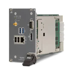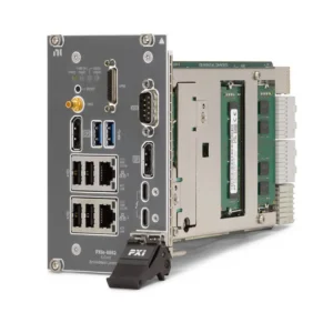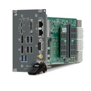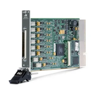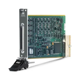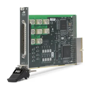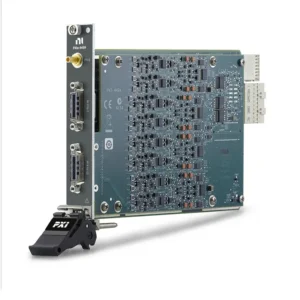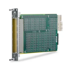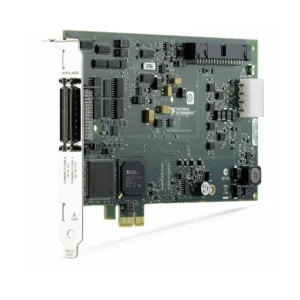


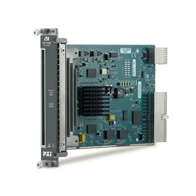


PXI-7954R Virtex-5 LX110 FlexRIO FPGA Module
Земля PXI-7954R, also commonly identified as the ПХИ-7954, is a PXI FPGA module for NI FlexRIO systems. It provides a user-programmable Xilinx Virtex-5 LX110 FPGA, 132 configurable FPGA I/O lines, 128 MB of onboard DRAM and three DMA channels for building customized high-speed measurement and control instruments.
The module connects to an interchangeable NI FlexRIO adapter module through a high-density card-edge interface. Depending on the selected adapter, the PXI-7954R can support high-speed analog input, analog output, digital waveform generation, digital protocol testing, image acquisition or other specialized measurement functions.
Unlike a fixed-function digitizer or digital I/O module, the PXI-7954R allows engineers to implement signal processing, custom triggering, protocol logic, filtering, control loops and data reduction directly in FPGA hardware using the LabVIEW FPGA Module.
Key Features of the PXI-7954R
- Xilinx Virtex-5 LX110 user-programmable FPGA
- 17,280 Virtex-5 FPGA slices
- 69,120 LUTs and flip-flops
- 64 DSP48 hardware multiplier slices
- 4,608 kbits of embedded block RAM
- 132 configurable FPGA I/O lines
- Up to 132 single-ended I/O channels
- Up to 66 differential I/O pairs
- 400 Mb/s maximum single-ended I/O rate
- 1 Gb/s maximum differential I/O rate
- Two 64 MB onboard DRAM banks
- 128 MB total onboard DRAM
- 800 MB/s theoretical DRAM bandwidth per bank
- Three DMA channels
- 40 MHz default FPGA timebase
- PXI trigger, PXI_CLK10 and PXI star-trigger support
- High-density FlexRIO adapter-module connector
- LabVIEW FPGA and NI-RIO software support
- Compatible with interchangeable FlexRIO adapter modules
PXI-7954R Technical Specifications
| Product Model | PXI-7954R |
|---|---|
| Alternative Model Name | ПХИ-7954 |
| Part Number | 780563-01 |
| Product Type | PXI FPGA module for FlexRIO |
| ФПГА | Xilinx Virtex-5 LX110 |
| FPGA Slices | 17,280 |
| LUTs and Flip-Flops | 69,120 |
| DSP48 Slices | 64 |
| DSP Multiplier Size | 25 × 18 bits |
| Embedded Block RAM | 4,608 kbits |
| General-Purpose FPGA I/O | 132 lines |
| Single-Ended Configuration | Up to 132 channels |
| Differential Configuration | Up to 66 differential pairs |
| Supported I/O Standards | 1.2 V, 1.5 V, 1.8 V, 2.5 V and 3.3 V, adapter dependent |
| Maximum Single-Ended I/O Rate | 400 Mb/s using LVDCI25 |
| Maximum Differential I/O Rate | 1 Gb/s using LVDS |
| I/O Banks | 4 |
| Bank 0 and Bank 2 | 32 single-ended channels per bank |
| Bank 1 and Bank 3 | 34 single-ended channels per bank |
| Global Clock Inputs | 1 LVTTL and 1 LVDS |
| Default FPGA Timebase | 40 MHz |
| Timebase Reference | PXI 10 MHz clock, PXI_CLK10 |
| Timebase Accuracy | ±100 ppm |
| Timebase Jitter | 250 ps peak-to-peak |
| DMA Channels | 3 |
| Supported Data Transfers | DMA, interrupts and programmed I/O |
| Onboard DRAM | 128 MB total |
| DRAM Configuration | 2 banks, 64 MB per bank |
| Theoretical DRAM Data Rate | 800 MB/s per bank |
| Connection Resources | PXI triggers, PXI_CLK10 and PXI star trigger |
| I/O Connector | High-density card-edge FlexRIO connector |
| Maximum Working Voltage | 0 V to 3.3 V, Measurement Category I |
| Шинный интерфейс | PXI master/slave interface |
| Operating Temperature | 0°C to 55°C |
| Storage Temperature | -20°C to 70°C |
| Operating Humidity | 10% to 90%, noncondensing |
| Maximum Altitude | 2,000 m at 25°C |
| Dimensions | 18.8 × 12.9 cm, excluding connectors |
| Weight | 190 g |
| Поддержка программного обеспечения | LabVIEW, LabVIEW FPGA Module and NI-RIO |
PXI-7954R Part Number and System Components
| Item | Part Number | Описание |
|---|---|---|
| PXI-7954R | 780563-01 | Virtex-5 LX110 PXI FPGA module for FlexRIO |
| FlexRIO Adapter Module | Model dependent | Provides application-specific analog, digital, RF or vision I/O |
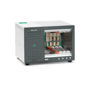
| PXI Шасси | Model dependent | Provides the PXI backplane, power, cooling and trigger resources |
| PXI Controller or MXI Interface | Model dependent | Runs the host application and communicates with the FPGA module |
| LabVIEW FPGA Module | License dependent | Compiles graphical FPGA code for the Virtex-5 LX110 device |
The PXI-7954R generally requires a compatible FlexRIO adapter module when external analog or digital signals must be connected. The FPGA module alone can also be used for onboard processing or certain FPGA-to-host applications that do not require external adapter I/O.
Virtex-5 LX110 FPGA Architecture
The PXI-7954R contains a Xilinx Virtex-5 LX110 FPGA. It is the largest FPGA offered in the original PXI-795xR FlexRIO family and provides more programmable logic than the PXI-7951R, PXI-7952R and PXI-7953R.
The FPGA includes 17,280 slices, represented in NI specifications as 69,120 LUTs and flip-flops. These resources can implement parallel state machines, triggering logic, counters, protocol engines, filters and custom data-processing pipelines.
Because the FPGA executes operations in dedicated hardware, multiple functions can run simultaneously without depending on sequential operating-system execution.
64 DSP48 Slices
The Virtex-5 LX110 provides 64 DSP48 slices with dedicated 25 × 18-bit multiplier resources. These blocks can accelerate multiply-and-accumulate operations used in digital signal processing.
Typical FPGA DSP functions include:
- Finite impulse response filtering
- Infinite impulse response filtering
- Digital downconversion
- Signal averaging
- Scaling and calibration correction
- Correlation and pattern detection
- Real-time control calculations
The number of DSP blocks required depends on word length, clock rate, filter structure and whether the FPGA design reuses arithmetic resources across clock cycles.
Embedded FPGA Block RAM
The PXI-7954R provides 4,608 kbits of FPGA block RAM. Block RAM is located inside the FPGA and offers deterministic, low-latency storage for FIFOs, lookup tables, temporary buffers and processing states.
Block RAM is particularly useful when data must be accessed within a few FPGA clock cycles. Larger waveform records should normally be stored in the external onboard DRAM.
128 MB Onboard DRAM
The module contains two independent 64 MB DRAM banks, providing 128 MB of total onboard memory. Each bank offers a theoretical maximum data rate of 800 MB/s between the DRAM and FPGA.
Onboard DRAM can store acquired waveforms, generated patterns, image data or intermediate processing results. Separating data across two banks can allow one memory bank to support acquisition while the other is used for processing or generation.
The 800 MB/s specification applies to the theoretical FPGA-to-DRAM interface for each memory bank. It should not be interpreted as the sustained transfer rate across the traditional PXI host bus.
Three DMA Channels
The PXI-7954R provides three DMA channels for transferring data between the FPGA and host controller. DMA transfers reduce processor involvement and are suitable for continuous or block-based waveform transfer.
An FPGA application can assign separate DMA FIFOs to different types of information, such as acquired samples, processed results and configuration data. The total host throughput remains subject to the PXI bus, controller and software architecture.
132 Configurable FPGA I/O Lines
The FlexRIO interface provides 132 general-purpose FPGA I/O lines divided across four FPGA banks. The lines can be configured as 132 single-ended channels, 66 differential pairs or a combination of both.
Banks 0 and 2 each contain 32 single-ended channels. Banks 1 and 3 each contain 34 single-ended channels. The attached FlexRIO adapter module determines which FPGA signals and electrical standards are available to the external system.
Single-Ended and Differential Data Rates
The PXI-7954R supports single-ended FPGA I/O rates up to 400 Mb/s when using the applicable LVDCI25 standard. Differential LVDS connections can operate at rates up to 1 Gb/s.
These are FPGA interface capabilities. The maximum usable sample rate or data rate of a complete FlexRIO instrument also depends on the adapter module, FPGA design, signal integrity, clocking and external cabling.
Supported I/O Voltage Standards
Depending on the FPGA configuration and attached adapter module, the I/O banks can support 1.2 V, 1.5 V, 1.8 V, 2.5 V and 3.3 V signaling standards.
Do not connect signals directly to the high-density card-edge interface unless the electrical design follows the applicable FlexRIO and Xilinx requirements. Voltage compatibility, termination, drive strength and bank power must be verified before compiling and running a custom FPGA design.
Interchangeable FlexRIO Adapter Modules
A FlexRIO system combines the PXI-7954R FPGA carrier with an application-specific adapter module. The adapter contains the analog or digital front-end circuitry required by the measurement application.
Available adapter types can provide:
- High-speed analog input
- High-speed analog output
- High-speed digital I/O
- Camera and image-acquisition interfaces
- RF and intermediate-frequency signal conversion
- Custom electrical interfaces
The adapter module determines channel count, connector type, voltage range, analog bandwidth, ADC or DAC resolution and external signal-protection specifications.
FlexRIO Adapter Compatibility
Compatibility must be checked for the exact adapter model and PXI-7954R hardware revision. Some newer or high-speed adapter modules require a particular revision of the FPGA module.
For example, certain versions of the NI-5752B Digitizer Adapter Module require revision C or later when used with PXI-795xR FPGA modules. Confirm the board revision, adapter compatibility and required software version before ordering a replacement module.
Custom Triggering and Decision Logic
Trigger conditions can be implemented directly in the FPGA rather than being limited to the fixed trigger functions of a conventional instrument. The FPGA can monitor several signals simultaneously and generate a trigger when a custom logical or timing condition occurs.
Possible conditions include a specific digital pattern, threshold crossing, pulse sequence, protocol command or combination of several measurement events.
Real-Time Signal Processing
FPGA processing can reduce the quantity of data transferred to the PXI controller. Instead of sending every raw sample, the FPGA can filter, average, decimate or analyze data and transfer only relevant results.
This is valuable when the adapter produces data faster than the traditional PXI bus can continuously transfer to the controller. Local processing and event detection allow the system to retain important information while reducing host bandwidth requirements.
Deterministic Control
The PXI-7954R can implement deterministic control functions with timing defined by FPGA clock cycles. The FPGA does not depend on Windows task scheduling and can respond to I/O events with predictable latency.
Applications can include hardware-in-the-loop interfaces, machine control, actuator testing, closed-loop research systems and custom safety-monitoring logic.
40 MHz Default Timebase
The default FPGA timebase operates at 40 MHz. Engineers can derive additional clocks within the FPGA design when supported by the clocking resources and adapter module.
The PXI-7954R can reference the chassis PXI_CLK10 signal. It also has access to PXI trigger lines and the PXI star trigger for coordination with other instruments in the chassis.
PXI Trigger Integration
PXI backplane triggers allow the FPGA module to exchange timing and event signals with digitizers, waveform generators, data acquisition modules and other PXI instruments.
The PXI star trigger provides a dedicated slot-to-system-timing connection with closely matched routing. Exact synchronization performance depends on the chassis, system timing architecture and FPGA code.
LabVIEW FPGA Programming
The PXI-7954R is programmed using the LabVIEW FPGA Module. Engineers create FPGA logic graphically, compile it for the Virtex-5 LX110 device and download the generated bitfile to the module.
LabVIEW FPGA supports parallel loops, state machines, fixed-point arithmetic, memory interfaces, DMA FIFOs and direct control of adapter-module I/O. Compilation can take substantial time because the design must be synthesized, placed and routed for the physical FPGA.
NI-RIO Driver Support
The NI-RIO driver provides communication between the host application and FPGA hardware. Host software can read and write front-panel controls, transfer data through DMA FIFOs and execute FPGA invoke methods.
The PXI-7954R is a legacy FlexRIO module, so operating-system, LabVIEW, FPGA compiler and NI-RIO compatibility should be verified before changing or upgrading the existing software environment.
LabVIEW Real-Time Integration
The optional LabVIEW Real-Time Module can be used when a PXI real-time controller manages the FlexRIO system. The FPGA handles the fastest and most deterministic I/O operations, while the real-time controller performs test sequencing, supervisory control, communication and data logging.
This layered architecture allows engineers to place each function on the processing target that best matches its timing and computational requirements.
Coprocessing Applications
The PXI-7954R can be used as a hardware coprocessor even when an external adapter module is not required. Computationally intensive algorithms can execute in FPGA hardware while the PXI controller handles the application interface and higher-level logic.
Possible coprocessing functions include pattern matching, digital filtering, data compression, custom encoding and deterministic event detection.
High-Speed Digitizer Systems
When paired with a compatible digitizer adapter, the PXI-7954R can acquire analog signals and process samples directly in the FPGA. The FPGA can implement triggering, filtering, averaging, digital downconversion or custom spectral processing.
Related digitizer adapters include the NI-5734 High-Speed Digitizer Adapter Module and compatible NI-575x FlexRIO adapters.
Digital Protocol Testing
A digital adapter module allows the FPGA to generate, acquire or analyze custom digital protocols. Engineers can implement protocol timing, framing, parity checking, error injection and device-specific command sequences directly in hardware.
This is useful when a standard digital instrument does not support the required protocol or timing behavior.
Image Acquisition and Processing
Compatible camera adapter modules can turn the PXI-7954R into a custom image-acquisition and processing instrument. FPGA logic can process pixel data as it arrives, performing operations such as thresholding, filtering, region detection and data reduction.
Real-time FPGA image processing can reduce controller workload and avoid transferring every raw image when only extracted measurements are required.
Hardware-in-the-Loop Testing
The PXI-7954R is suitable for hardware-in-the-loop systems that require custom digital interfaces, precise timing or low-latency signal processing. FPGA logic can simulate sensors, decode controller outputs and generate responses within deterministic timing constraints.
When combined with a real-time controller, the FPGA can manage high-speed electrical interfaces while the controller runs the plant model and test sequence.
Typical PXI-7954R Applications
- Custom high-speed instrumentation
- High-speed analog data acquisition
- Digital waveform generation and acquisition
- Protocol-aware digital testing
- Симуляция с аппаратным входом
- Real-time signal processing
- FPGA-based triggering
- Digital filtering and decimation
- Image acquisition and processing
- Software-defined radio research
- Radar and communications research
- Particle and scientific instrumentation
- Замкнутая система управления
- Automated electronic validation
- FPGA hardware coprocessing
PXI-7954R Development Workflow
Step 1: Select the Adapter Module
Choose the FlexRIO adapter that provides the required analog, digital, RF or vision interface. Verify its compatibility with the PXI-7954R revision.
Step 2: Install the Software
Install a compatible LabVIEW version, LabVIEW FPGA Module, NI-RIO driver and the applicable FlexRIO Adapter Module Support package.
Step 3: Install the Hardware
Power off the chassis, install the PXI-7954R in a compatible PXI or hybrid slot and attach the adapter module using its guide pins and captive screws.
Step 4: Create the FPGA VI
Implement the required acquisition, generation, triggering, processing and control functions in LabVIEW FPGA.
Step 5: Compile the FPGA Design
Compile the FPGA VI for the Virtex-5 LX110 target. Review timing and resource reports to confirm that the design meets the required FPGA clock rate.
Step 6: Develop the Host Application
Create a LabVIEW, LabVIEW Real-Time or supported host application to configure the FPGA, transfer data and display or store measurement results.
Step 7: Validate the Complete System
Verify signal voltage, timing, clocking, DMA throughput, DRAM operation and adapter-module performance under the expected operating conditions.
PXI-7954R Troubleshooting
The module is not detected in NI MAX
Confirm that the module is fully inserted into a supported PXI or hybrid slot. Check chassis power, controller communication and NI-RIO installation. The FPGA carrier appears under RIO Devices, but the attached adapter may not appear as a separate device in NI MAX.
The FPGA VI does not compile
Verify that the correct PXI-7954R target and compatible FPGA compilation tools are installed. Review the compiler report for timing violations, excessive resource use or unsupported functions.
The FPGA design exceeds available resources
Reduce parallel logic, reuse arithmetic functions, decrease buffer sizes or move non-time-critical processing to the host. Pay particular attention to LUT, block RAM and DSP48 utilization.
The adapter module does not operate
Confirm adapter compatibility, FPGA module revision, adapter support software and CLIP configuration. Inspect the card-edge connector and ensure that the adapter’s captive screws are secured.
DMA data transfer stops or overflows
Check the FPGA FIFO depth, host read rate and PXI controller workload. Use onboard DRAM or FPGA data reduction when the raw data rate exceeds sustained host-transfer capability.
DRAM data is corrupted
Review the DRAM addressing, arbitration and clock-domain-crossing logic. Ensure that reads and writes remain within the selected 64 MB memory bank and follow the required interface timing.
Digital data contains errors
Verify the I/O voltage standard, termination, cable impedance, clock alignment and adapter specifications. High-speed digital interfaces require careful signal-integrity design.
The FPGA timing requirement is not met
Pipeline long combinational paths, reduce arithmetic word length, add registers between processing stages or lower the requested FPGA clock rate.
The FPGA bitfile cannot run after a software upgrade
Legacy FlexRIO devices may require specific combinations of LabVIEW, LabVIEW FPGA, NI-RIO and compilation tools. Check the compatibility of the entire software stack before upgrading a production system.
PXI-7954R Comparison with Similar FlexRIO FPGA Modules
| Модель | ФПГА | DSP Slices | Block RAM | Onboard DRAM |
|---|---|---|---|---|
| PXI-7951R | Virtex-5 LX30 | 32 | 1,152 kbits | Ничего |
| PXI-7952R | Virtex-5 LX50 | 48 | 1,728 kbits | 128 MB |
| PXI-7953R | Virtex-5 LX85 | 48 | 3,456 kbits | 128 MB |
| PXI-7954R | Virtex-5 LX110 | 64 | 4,608 kbits | 128 MB |
| PXIe-7962R | Virtex-5 SX50T | 288 | 4,752 kbits | 512 MB |
| PXIe-7966R | Virtex-5 SX95T | 640 | 8,784 kbits | 512 MB |
PXI-7954R vs PXI-7953R
Земля PXI-7953R uses a Virtex-5 LX85 FPGA with fewer LUTs, flip-flops, DSP slices and block RAM. Both modules provide 128 MB of onboard DRAM and three DMA channels.
Choose the PXI-7954R when the FPGA application requires additional parallel logic, larger internal buffers or more DSP resources. The PXI-7953R may be sufficient for designs with lower resource requirements.
PXI-7954R vs PXIe-7966R
Земля PXIe-7966R uses a Virtex-5 SX95T FPGA with substantially more DSP slices, 512 MB of DRAM, 16 DMA channels and a PXI Express ×4 interface.
The PXIe-7966R is better suited to processing-intensive and high-throughput systems. The PXI-7954R is appropriate for existing PXI installations and applications designed around its Virtex-5 LX110 FPGA and legacy FlexRIO software environment.
Recommended Related Products
- PXI-7951R FlexRIO FPGA Module
- PXI-7952R FlexRIO FPGA Module
- PXI-7953R FlexRIO FPGA Module
- PXIe-7961R FlexRIO FPGA Module
- PXIe-7962R FlexRIO FPGA Module
- PXIe-7965R FlexRIO FPGA Module
- PXIe-7966R FlexRIO FPGA Module
- NI-5734 High-Speed Digitizer Adapter Module
- NI-5752B Digitizer Adapter Module
- NI-6584 High-Speed Digital Adapter Module
- View More NI PXI and PXI Express Modules
Selecting the Right FlexRIO FPGA Module
Choose the PXI-7954R when maintaining an existing PXI FlexRIO system that requires the Virtex-5 LX110 FPGA, 128 MB of DRAM and compatibility with a validated PXI-795xR application.
Select a smaller PXI-795xR model when the FPGA design uses fewer logic resources. Consider a PXI Express FlexRIO module when higher host throughput, more DMA channels, additional DRAM or greater DSP capacity is required.
Before replacing an FPGA carrier, confirm the adapter model, FPGA module revision, compiled bitfile target, PXI slot type and supported software versions.
Why Choose the PXI-7954R?
- Provides the largest FPGA in the PXI-795xR family
- Supports custom hardware-timed measurement functions
- Offers 132 configurable FPGA I/O lines
- Supports single-ended and differential signaling
- Includes 128 MB of onboard DRAM
- Provides three DMA channels for host communication
- Supports interchangeable FlexRIO adapter modules
- Implements real-time processing directly in FPGA hardware
- Integrates with PXI triggers and the PXI star trigger
- Supports LabVIEW FPGA and NI-RIO development
Frequently Asked Questions
What is the PXI-7954R?
The PXI-7954R is a user-programmable PXI FPGA carrier module for NI FlexRIO systems. It combines a Virtex-5 LX110 FPGA with configurable I/O, onboard DRAM and DMA communication.
Is PXI-7954 the same as PXI-7954R?
PXI-7954 is commonly used as a shortened name, but the official NI model is PXI-7954R. The “R” identifies it as reconfigurable FPGA hardware.
Which FPGA does the PXI-7954R use?
It uses a Xilinx Virtex-5 LX110 FPGA with 17,280 slices, 64 DSP48 slices and 4,608 kbits of embedded block RAM.
How many FPGA I/O lines are available?
The module provides 132 configurable I/O lines. They can be configured as as many as 132 single-ended channels, 66 differential pairs or a mixture of both.
What are the maximum digital I/O rates?
The FPGA interface supports rates up to 400 Mb/s for applicable single-ended configurations and 1 Gb/s for differential LVDS configurations.
Does the PXI-7954R include analog inputs?
No fixed analog inputs are built into the FPGA carrier. Analog measurement capabilities are determined by the attached FlexRIO adapter module.
Does it require a FlexRIO adapter module?
An adapter module is generally required for external analog or digital I/O. The FPGA carrier can be used without an adapter for certain coprocessing applications.
How much onboard DRAM is provided?
The module provides 128 MB of onboard DRAM divided into two 64 MB banks. Each bank has a theoretical FPGA-interface bandwidth of 800 MB/s.
How many DMA channels are available?
The PXI-7954R provides three DMA channels for transferring data between the FPGA and host controller.
Does the PXI-7954R support peer-to-peer streaming?
The PXI-7954R uses the traditional PXI bus and does not provide the PXI Express peer-to-peer streaming capabilities available on certain PXIe FlexRIO modules.
Which software is required?
A typical development system requires LabVIEW, the LabVIEW FPGA Module, NI-RIO and the applicable FlexRIO Adapter Module Support package. LabVIEW Real-Time is optional.
What is the PXI-7954R part number?
The standard NI part number for the PXI-7954R is 780563-01.
Can an existing compiled bitfile run on another FlexRIO FPGA model?
An FPGA bitfile is compiled for a specific FPGA target. A design created for the PXI-7954R normally must be recompiled before it can run on a different FlexRIO FPGA module.
Request a Quote for the PXI-7954R
Contact us for current availability, lead time and project pricing for the PXI-7954R Virtex-5 LX110 FlexRIO FPGA Module. Please provide the required adapter-module model and FPGA hardware revision when requesting a quotation. We can also help identify compatible PXI chassis, FlexRIO adapters and related FPGA modules for your test system.