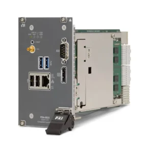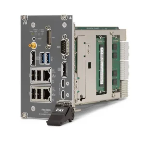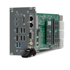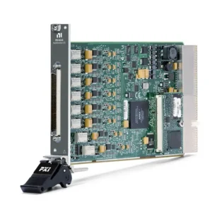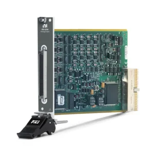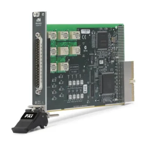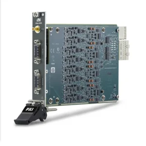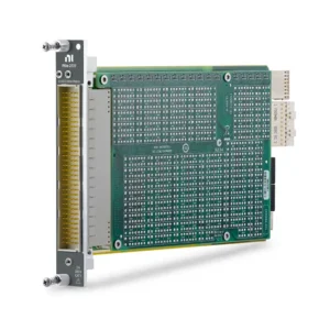


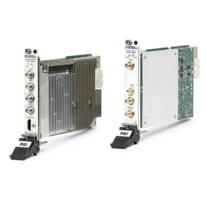
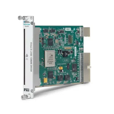
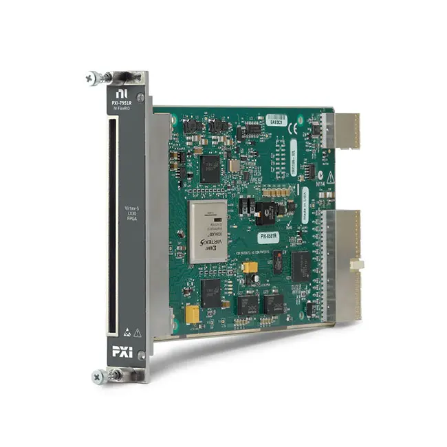
PXI-7951R Virtex-5 LX30 FPGA FlexRIO Module
Земля PXI-7951R is a National Instruments FlexRIO FPGA module designed for custom high-speed digital I/O, inline signal processing, protocol implementation and automated test applications. It combines a user-programmable Xilinx Virtex-5 LX30 FPGA with an interface for compatible NI FlexRIO adapter modules.
The module provides 66 differential or 132 single-ended general-purpose I/O connections through its adapter-module interface. Depending on the attached adapter and signal configuration, it supports data rates up to 1 Gb/s per LVDS pair or 400 Mb/s per single-ended channel.
The PXI-7951R does not include onboard DRAM. Applications therefore use the FPGA’s embedded block RAM or transfer data between the FPGA and host controller through three DMA channels. This configuration is suitable for FPGA processing and control applications that do not require large local acquisition buffers.
Key Features of the PXI-7951R
- Xilinx Virtex-5 LX30 user-programmable FPGA
- 4,800 FPGA slices
- 19,200 lookup tables and flip-flops
- 32 DSP48 multiplier and processing slices
- 1,152 kbits of embedded block RAM
- 66 differential or 132 single-ended I/O channels
- Up to 1 Gb/s per LVDS differential pair
- Up to 400 Mb/s per single-ended channel
- Three host DMA channels
- 40 MHz default FPGA timebase
- PXI_CLK10 reference-clock support
- Compatible with interchangeable FlexRIO adapter modules
- Programmable using the LabVIEW FPGA Module
- Conventional PXI bus interface
- No onboard DRAM
PXI-7951R Technical Specifications
| Product Model | PXI-7951R |
|---|---|
| Part Number | 780560-01 |
| Product Type | FlexRIO FPGA module for PXI |
| ФПГА | Xilinx Virtex-5 LX30 |
| FPGA Slices | 4,800 |
| Lookup Tables and Flip-Flops | 19,200 |
| DSP Resources | 32 DSP48 slices with 25 × 18 multipliers |
| Embedded Block RAM | 1,152 kbits |
| Onboard DRAM | Ничего |
| Differential I/O | 66 pairs |
| Single-Ended I/O | 132 channels |
| Maximum LVDS Data Rate | Up to 1 Gb/s per differential pair |
| Maximum Single-Ended Data Rate | Up to 400 Mb/s per channel |
| DMA Channels | 3 |
| Default FPGA Timebase | 40 MHz |
| Reference Clock | PXI_CLK10 |
| Timebase Accuracy | ±100 ppm |
| Timebase Jitter | 250 ps peak-to-peak |
| Approximate Host Streaming Throughput | Up to 130 MB/s, application dependent |
| Шинный интерфейс | Conventional PXI |
| Module Dimensions | Approximately 18.8 × 13.0 cm (7.4 × 5.1 in.) |
| Programming Environment | LabVIEW FPGA with a compatible NI-RIO driver |
| Lifecycle Status | Discontinued |
| Recommended Replacement | PXIe-7976R |
PXI-7951R Part Number
| Item | Part Number | Описание |
|---|---|---|
| PXI-7951R | 780560-01 | Virtex-5 LX30 FlexRIO FPGA module with 66 differential I/O pairs |
The PXI-7951R is an FPGA carrier module and normally requires a compatible FlexRIO adapter module to provide the physical analog, digital, RF or communication interface required by the application. Confirm adapter-module compatibility, software support and required cabling before ordering.
Virtex-5 LX30 FPGA Architecture
The PXI-7951R uses a Xilinx Virtex-5 LX30 FPGA that can be programmed to perform application-specific hardware operations. Unlike processor-based software, FPGA logic executes through parallel hardware resources, allowing multiple acquisition, processing and control tasks to run concurrently.
The FPGA provides 4,800 slices, 19,200 lookup tables and flip-flops, 32 DSP48 slices and 1,152 kbits of embedded block RAM. These resources can implement digital filters, counters, triggers, state machines, custom protocols and real-time decision logic.
The LX30 is the smallest FPGA in the PXI-795xR family. It is appropriate for applications with moderate logic and signal-processing requirements. Designs requiring additional DSP blocks, block RAM or parallel logic should be evaluated for a larger FlexRIO FPGA target.
FlexRIO Adapter Module Interface
The FlexRIO architecture separates the programmable FPGA carrier from the application-specific I/O circuitry. The PXI-7951R provides the FPGA and PXI communication resources, while an interchangeable adapter module supplies the required connectors, transceivers, converters or signal conditioning.
This design allows the same FPGA module family to support high-speed digital interfaces, analog-to-digital converters, digital-to-analog converters, RF interfaces and custom adapter modules. The available sample rate, voltage range, signal standard and connector type depend primarily on the selected adapter.
The 66 differential pairs or 132 single-ended signals describe the electrical interface between the FPGA module and adapter. They should not be treated as directly accessible front-panel I/O unless the installed adapter exposes them in that form.
66 Differential or 132 Single-Ended I/O Channels
The PXI-7951R supports as many as 66 differential general-purpose I/O pairs. These pairs can support LVDS signaling at rates up to 1 Gb/s per pair when used with compatible circuitry and an appropriate FPGA design.
The interface can alternatively provide as many as 132 single-ended channels at data rates up to 400 Mb/s per channel. Actual performance depends on the adapter module, FPGA timing, signal standard, connector, cable and test-fixture layout.
Engineers can configure FPGA resources to create custom input, output or bidirectional interfaces. This flexibility makes the module useful for proprietary digital buses and hardware protocols that are not supported by conventional fixed-function instruments.
Three DMA Channels
Three DMA channels support data movement between the FPGA and host controller. FPGA DMA FIFOs can be used for continuous acquisition, waveform generation, processed-data transfer and command or status communication.
The achievable transfer rate depends on the PXI controller, chassis, DMA configuration, data width and activity from other instruments. Because the PXI-7951R uses a conventional PXI bus, it does not provide the higher throughput or peer-to-peer streaming capabilities available from later PXI Express FlexRIO modules.
Efficient FPGA applications often process or reduce data before transferring it to the host. Decimation, filtering, event detection and packet selection can reduce PXI bandwidth requirements.
No Onboard DRAM
The PXI-7951R does not include external onboard DRAM. Temporary values, delay lines, lookup tables and small buffers must fit within the FPGA’s 1,152 kbits of embedded block RAM unless they are transferred to host memory.
This design works well for low-latency processing, digital control and streaming applications where large local buffers are unnecessary. It is less suitable for applications that must capture or generate long bursts at full adapter-module rate without immediate host transfer.
For buffered acquisition or generation, consider a FlexRIO module with onboard DRAM. The PXI-7952R, PXI-7953R and PXI-7954R each provide 128 MB of DRAM, while newer PXI Express models offer substantially greater memory capacity.
FPGA-Based Signal Processing
The 32 DSP48 slices can perform multiply-and-accumulate operations used in finite impulse response filters, control algorithms, channel scaling, mixing and other mathematical functions. FPGA processing can operate directly on incoming data before results are sent to the host.
Processing data on the FPGA reduces software latency and can lower the amount of data transferred across the PXI bus. The achievable processing rate depends on algorithm complexity, fixed-point word length, pipelining and FPGA resource utilization.
Deterministic Timing and Triggering
FPGA logic provides deterministic hardware timing for triggers, pulse generation, protocol control and measurement sequencing. The default FPGA timebase is 40 MHz, and the PXI-7951R can use the PXI_CLK10 backplane clock as a reference source.
Engineers can implement custom timing relationships, edge detection, counters and state machines directly in the FPGA fabric. This is useful when software-controlled timing is not sufficiently fast or repeatable.
Custom Digital Protocols
The PXI-7951R can implement proprietary and nonstandard digital protocols using FPGA logic. Developers can define framing, encoding, checksums, handshaking, triggers and error-insertion behavior according to the device under test.
The electrical signaling remains dependent on the attached adapter module. Voltage-level translation, termination and physical connectors must match the target interface.
Inline Data Processing
Incoming data can be processed immediately in hardware rather than transferred unmodified to the host. The FPGA can perform threshold detection, digital filtering, averaging, protocol decoding and event qualification with predictable latency.
Only processed measurements or selected events need to be transferred through DMA. This approach can make efficient use of the conventional PXI bus when adapter-side data rates exceed sustained host-transfer capacity.
Hardware-in-the-Loop Testing
The PXI-7951R can perform deterministic stimulus generation and response capture in hardware-in-the-loop systems. FPGA logic can emulate sensor signals, monitor controller outputs and react to detected events without waiting for a host-software loop.
Its exact I/O capabilities depend on the adapter module. Before using the product with automotive, aerospace or industrial controllers, confirm voltage ranges, isolation, protection and timing requirements for the complete interface.
Custom FlexRIO Adapter Development
The PXI-7951R can be paired with a custom FlexRIO adapter designed around the required converters, connectors and interface circuitry. This allows engineers to build specialized FPGA instruments that are not available as standard products.
Custom adapter design requires careful attention to FlexRIO electrical requirements, clocking, power consumption, signal integrity and FPGA pin assignments. NI’s adapter module development resources should be consulted before producing custom hardware.
LabVIEW FPGA Programming
The FPGA is programmed using a compatible version of the LabVIEW FPGA Module and NI-RIO driver. LabVIEW FPGA code is compiled into a hardware bitfile that runs directly on the Virtex-5 device.
The host application can communicate with FPGA controls, indicators, interrupts and DMA FIFOs through the NI-RIO interface. Existing systems should preserve compatible development software, drivers and compiled bitfiles because support for this discontinued module may not be included in current software releases.
Typical PXI-7951R Applications
- Custom high-speed digital interfaces
- Proprietary protocol implementation
- Digital signal processing
- Симуляция с аппаратным входом
- Deterministic triggering and control
- Inline data filtering and event detection
- High-speed pattern generation
- Digital waveform acquisition
- Bit-error-rate testing
- Communications research
- Production test systems
- Custom instrumentation development
PXI-7951R Troubleshooting
The PXI-7951R Is Not Detected
Confirm that the module is fully installed in a compatible PXI slot and that the chassis and controller are powered correctly. Verify that an NI-RIO driver version supporting the PXI-7951R is installed, then inspect the system in NI Measurement & Automation Explorer.
The FPGA Bitfile Does Not Load
Confirm that the bitfile was compiled specifically for the PXI-7951R and the installed adapter module. A bitfile created for another FlexRIO FPGA target may use different FPGA resources, pin assignments or interface definitions.
The FPGA Design Does Not Compile
Review FPGA resource utilization, timing constraints and unsupported functions. The Virtex-5 LX30 offers fewer logic, DSP and memory resources than larger PXI-795xR models. Reduce parallel processing, reuse arithmetic resources or move appropriate operations to the host.
A High-Speed Interface Produces Data Errors
Check the adapter module, signal standard, termination, clock alignment, cable length and test-fixture impedance. Validate FPGA timing closure and confirm that the requested data rate is supported by every component in the signal path.
DMA Transfer Is Slower Than Expected
Review the DMA FIFO width, transfer-block size, host read frequency and controller performance. Conventional PXI bandwidth is shared, so other installed modules can reduce the throughput available to the PXI-7951R.
DMA FIFO Overflow Occurs
Reduce the FPGA data rate, increase the DMA FIFO allocation or transfer data in larger blocks. FPGA filtering, decimation and event selection can reduce the amount of information sent to the host.
The Design Requires More Buffer Memory
The PXI-7951R has no onboard DRAM. If the design cannot fit within embedded block RAM and continuous host streaming is insufficient, use a FlexRIO FPGA module with external DRAM.
The Adapter Module Is Not Recognized
Confirm that the adapter is compatible with the PXI-7951R and that the FPGA project contains the correct adapter definition. Inspect the connector for bent contacts and verify that the adapter is fully secured before applying power.
PXI-7951R Comparison with Related FlexRIO Modules
| Модель | ФПГА | FPGA Resources | Onboard DRAM | Best Suited For |
|---|---|---|---|---|
| PXI-7951R | Virtex-5 LX30 | 4,800 slices, 32 DSP48, 1,152 kbits BRAM | Ничего | Moderate FPGA processing without large local buffers |
| PXI-7952R | Virtex-5 LX50 | 7,200 slices, 48 DSP48, 1,728 kbits BRAM | 128 MB | Buffered acquisition and larger FPGA designs |
| PXI-7953R | Virtex-5 LX85 | 12,960 slices, 48 DSP48, 3,456 kbits BRAM | 128 MB | Complex logic and higher-capacity processing |
| PXI-7954R | Virtex-5 LX110 | 17,280 slices, 64 DSP48, 4,608 kbits BRAM | 128 MB | Largest FPGA designs in the conventional PXI family |
| PXIe-7976R | Kintex-7 410T | 63,550 slices, 1,540 DSP48, 28,620 kbits BRAM | 2 GB | Modern high-throughput FlexRIO systems and migration |
PXI-7951R vs PXI-7952R
The PXI-7951R uses a Virtex-5 LX30 FPGA and has no onboard DRAM. The PXI-7952R uses a larger Virtex-5 LX50 FPGA and includes 128 MB of DRAM.
Choose the PXI-7951R for smaller FPGA applications that can stream data continuously or operate within embedded block RAM. Choose the PXI-7952R when additional logic, DSP resources and acquisition buffering are required.
PXI-7951R vs PXI-7953R
Земля PXI-7953R provides substantially more logic and block RAM than the PXI-7951R while also including 128 MB of onboard DRAM. It is better suited to larger parallel algorithms and buffered high-speed acquisition.
The PXI-7951R can remain a cost-effective option for maintaining validated systems whose compiled FPGA designs fit comfortably within the LX30 device.
PXI-7951R vs PXIe-7976R
Земля PXIe-7976R is the recommended modern replacement for the PXI-7951R. It uses a much larger Kintex-7 410T FPGA, includes 2 GB of onboard DRAM and supports PXI Express data transfer at rates up to 3.2 GB/s.
Migration is not necessarily a direct hardware substitution. The newer FPGA target has different resources, timing characteristics, software requirements and chassis-interface requirements. Existing FPGA code, adapter compatibility and test-system validation should be reviewed before replacement.
Recommended Related Products
- PXI-7952R Virtex-5 LX50 FlexRIO FPGA Module
- PXI-7953R Virtex-5 LX85 FlexRIO FPGA Module
- PXI-7954R Virtex-5 LX110 FlexRIO FPGA Module
- PXIe-7976R Kintex-7 FlexRIO FPGA Module
- NI-6581 High-Speed Digital FlexRIO Adapter Module
- View More NI PXI and PXI Express Modules
Selecting the Right FlexRIO FPGA Module
Choose the PXI-7951R when maintaining a conventional PXI FlexRIO system that uses a Virtex-5 LX30 target and does not require onboard DRAM. It provides sufficient resources for moderate custom digital interfaces, hardware timing and inline processing.
Select a PXI-7952R, PXI-7953R or PXI-7954R when the application requires larger FPGA resources or 128 MB of onboard DRAM. For new systems requiring greater processing capacity, larger buffers and faster host transfer, consider the PXIe-7976R or another current PXI Express FlexRIO module.
Why Choose the PXI-7951R?
- Maintains compatibility with validated Virtex-5 FlexRIO systems
- Provides a user-programmable LX30 FPGA
- Supports 66 differential or 132 single-ended signals
- Supports LVDS rates up to 1 Gb/s per pair
- Provides deterministic hardware processing and control
- Includes three DMA channels for host communication
- Works with compatible interchangeable FlexRIO adapters
- Supports custom protocols and inline signal processing
- Integrates with LabVIEW FPGA and NI-RIO
Frequently Asked Questions
What Is the PXI-7951R?
The PXI-7951R is a conventional PXI FlexRIO FPGA module featuring a user-programmable Xilinx Virtex-5 LX30 FPGA and an interface for compatible FlexRIO adapter modules.
What Is the PXI-7951R Part Number?
The standard NI part number for the PXI-7951R is 780560-01.
How Many I/O Channels Does It Provide?
The adapter interface supports as many as 66 differential pairs or 132 single-ended channels. The accessible signals and electrical characteristics depend on the installed adapter module.
What Is the Maximum LVDS Data Rate?
The interface supports rates up to 1 Gb/s per LVDS differential pair when used with compatible hardware and a suitable FPGA implementation.
Does the PXI-7951R Have Onboard DRAM?
No. The PXI-7951R has no onboard DRAM. It provides 1,152 kbits of embedded FPGA block RAM and can transfer data to host memory using DMA.
How Many DMA Channels Are Available?
The module provides three DMA channels for data communication between the FPGA and host controller.
Can the PXI-7951R Be Used Without an Adapter Module?
The carrier can be installed and programmed, but a compatible FlexRIO adapter module is normally required to provide usable external I/O connectors and application-specific signal conditioning.
Which Software Programs the FPGA?
The PXI-7951R is programmed using a compatible LabVIEW FPGA Module and NI-RIO driver. Verify legacy software support before configuring a replacement or refurbished system.
Is the PXI-7951R Still Available from NI?
No. The PXI-7951R has been discontinued. Availability is generally limited to refurbished, surplus and previously owned inventory.
What Is the Recommended PXI-7951R Replacement?
NI identifies the PXIe-7976R as the recommended replacement. The replacement uses PXI Express and offers a larger FPGA, substantially more memory and greater data-transfer performance.
Request a Quote for the PXI-7951R
Contact us for current availability, condition, lead time and project pricing for the PXI-7951R Virtex-5 LX30 FlexRIO FPGA Module. We can also help identify compatible FlexRIO adapter modules, PXI chassis and migration options for discontinued FPGA-based test systems.