






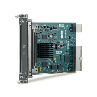
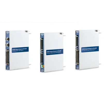
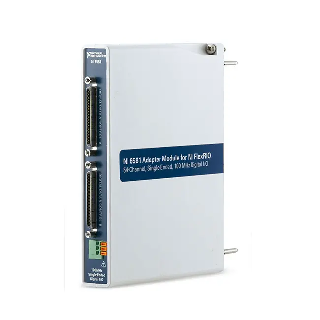
Product Introduction
Земля NI‑6581B является 100 MHz, 54-channel single-ended digital I/O adapter module for NI FlexRIO. It is designed for high-speed digital acquisition, digital waveform generation, device interface testing, custom protocol implementation and deterministic FPGA-based data processing.
When combined with a compatible FlexRIO FPGA module or Controller for FlexRIO, the NI‑6581B creates a programmable digital instrument capable of interfacing with digital devices through 48 bidirectional data channels and six programmable function interface channels.
The NI‑6581B is suitable for semiconductor validation, FPGA and ASIC testing, embedded system development, custom digital communication, hardware-in-the-loop testing, electronic design verification and automated production test applications.
Product Overview
Земля National Instruments NI‑6581B belongs to the NI FlexRIO digital adapter module family. Its standard part number is 783887‑01.
The module provides the electrical interface between a digital device under test and the user-programmable FPGA resources of a compatible FlexRIO system.
A typical system architecture is:
Digital DUT ↔ NI‑6581B ↔ FlexRIO FPGA Module ↔ PXI/PXIe System ↔ Host Application
The NI‑6581B handles single-ended digital signal acquisition and generation, while the associated FPGA implements timing, direction control, triggering, protocol processing, pattern generation, data reduction and host communication.
Key Features
54 Single-Ended Digital I/O Channels
The NI‑6581B provides 54 single-ended digital I/O channels across two digital data connectors.
The channel architecture includes:
- 48 bidirectional digital data channels
- Six programmable function interface channels
- Two external global clock inputs
- Two clock output terminals
This channel configuration supports parallel digital acquisition, waveform generation, device communication and application-specific control functions.
48 Bidirectional Data Channels
The 48 primary data channels are arranged as six 8-bit ports distributed across the two front-panel connectors.
Direction control is configurable by 8-bit port, allowing different groups of channels to perform input or output operations according to the FPGA application.
Bidirectional operation makes the NI‑6581B suitable for applications that require both device stimulation and response acquisition within the same programmable test system.
Six Programmable Function Interface Channels
In addition to the 48 data channels, the NI‑6581B provides six PFI channels, with three PFI lines available on each digital data connector.
These channels can participate in programmable control, handshaking, triggering and application-specific digital communication functions.
100 MHz Digital Operation
The NI‑6581B supports digital waveform operation at rates up to 100 MHz under supported voltage and system configurations.
This performance makes the module suitable for high-speed parallel digital buses, digital pattern generation, protocol emulation and electronic device validation.
Programmable Logic Voltage Support
The NI‑6581B supports commonly used digital voltage levels, including 1.8 V, 2.5 V and 3.3 V.
External power can also be supplied through the front-panel power connector when the DUT requires a supported externally referenced voltage. According to the device specifications, the external power source range is 1.8 V to 5.5 V, with 5 V operation requiring external power.
Each digital data connector can be referenced to an internal or external supply, providing additional flexibility when interfacing with devices that use different logic voltage requirements.
Two Global Clock Inputs
The NI‑6581B provides two global clock inputs, one on each digital data connector.
These clock inputs can connect an external sample clock to the global clock resources of the associated FlexRIO FPGA module for dynamic digital acquisition and synchronized operations.
Clock Output Capability
Each digital data connector includes a clock output terminal that can export a sample clock generated by the FlexRIO FPGA application.
This capability can be used to synchronize the connected DUT with FPGA-controlled acquisition or generation.
50 Ω Signal Architecture
The digital channels use nominal 50 Ω output impedance and 50 Ω characteristic-impedance traces.
Proper cable selection, termination, grounding and signal routing remain important when operating the module at high digital frequencies.
User-Programmable FPGA Processing
The NI‑6581B is designed to work with user-programmable FlexRIO FPGA hardware.
The FPGA can implement custom digital functions such as:
- Digital pattern generation
- Digital waveform acquisition
- Custom triggering
- Protocol generation and decoding
- Timing and sequencing
- Data framing
- State machines
- Error detection
- Real-time decision logic
- Data reduction and filtering
Technical Specifications
| Параметр | Спецификация |
|---|---|
| Product Type | FlexRIO Digital I/O Adapter Module |
| Модель | NI‑6581B |
| Part Number | 783887‑01 |
| Manufacturer | Национальные инструменты |
| Platform | NI FlexRIO |
| Signaling Type | Single-Ended Digital I/O |
| Total Digital I/O Channels | 54 |
| Bidirectional Data Channels | 48 |
| PFI Channels | 6 Total, 3 per Connector |
| Data Port Organization | Six 8-Bit Ports |
| Data Channel Direction Control | Configurable per 8-Bit Port |
| Maximum Toggle Rate | 100 MHz at ≥3.3 V |
| Internal Logic Voltage Levels | 1.8 V, 2.5 V and 3.3 V |
| External Power Source Range | 1.8 V to 5.5 V |
| Data Channel Output Impedance | 50 Ω Nominal |
| Characteristic Impedance | 50 Ω Traces |
| Absolute Maximum Input Range | −0.5 V to 6.5 V |
| External Global Clock Inputs | 2 |
| Clock Outputs | 2 |
| Digital Data Connectors | 2 × 68-Pin VHDCI |
| External Power Connector | Spring-Terminal Connector |
| FPGA Compatibility | Compatible NI FlexRIO FPGA Modules and Controllers for FlexRIO |
| Dimensions | 12.9 cm × 2.0 cm × 12.1 cm |
| Weight | 284 g |
| Operating Temperature | 0°C to 55°C |
| Storage Temperature | −20°C to 70°C |
| Primary Applications | Digital Interface Test, Custom Protocols, Semiconductor Validation and Automated Test |
How Does the NI‑6581B Work?
The NI‑6581B provides the physical single-ended digital interface between a DUT and a compatible NI FlexRIO FPGA.
A simplified signal path is:
Digital DUT ↔ NI‑6581B Digital Ports ↔ FlexRIO FPGA Logic ↔ DMA / PXI Express ↔ Host Software
During acquisition, incoming digital signals pass through the NI‑6581B interface and are transferred directly to the associated FPGA. The FPGA can perform deterministic triggering, pattern detection, protocol decoding or data reduction before transferring selected data to the host.
During generation, the FPGA creates digital patterns, timing sequences or protocol frames and sends them through the NI‑6581B to the connected DUT.
NI‑6581B Is a FlexRIO Adapter Module
The NI‑6581B is an адаптерный модуль and is not a complete standalone digital instrument.
A complete NI‑6581B system normally requires:
- NI‑6581B digital I/O adapter module
- Compatible FlexRIO FPGA module or Controller for FlexRIO
- Compatible PXI or PXIe chassis when using a PXI-based FlexRIO module
- Compatible PXI controller or host computer
- Appropriate VHDCI cables and connection accessories
- Compatible NI FlexRIO software
- FPGA application or supported instrument design
FlexRIO FPGA Integration
NI FlexRIO combines application-specific adapter modules with programmable FPGA hardware.
For the NI‑6581B, this architecture allows engineers to create custom digital instruments without designing a complete FPGA-connected physical interface from the beginning.
A typical acquisition architecture is:
Digital Input → NI‑6581B → FPGA Triggering and Protocol Processing → DMA → Host
A typical generation architecture is:
Host or FPGA Pattern → FPGA Timing Logic → NI‑6581B → Digital DUT
The exact channel behavior, timing architecture, trigger conditions and data processing functions depend on the FPGA design deployed to the compatible FlexRIO hardware.
Digital Port Architecture
The NI‑6581B includes two digital data connectors identified as DDCA and DDCB.
Each connector provides:
- 24 bidirectional data channels organized into three 8-bit ports
- Three programmable function interface channels
- One global clock input
- One clock output
- Ground and reserved terminals
Direction control for the primary data channels is configured per 8-bit port. Engineers should consider the required input and output grouping before assigning DUT signals to the connectors.
Digital Waveform Acquisition
The NI‑6581B can capture parallel digital signals and transfer them directly to FPGA logic for deterministic processing.
Potential acquisition functions include:
- Digital bus monitoring
- Pattern detection
- State monitoring
- Protocol analysis
- Event detection
- Timing verification
- Device response capture
- Trigger-qualified recording
FPGA processing can reduce the amount of data transferred to the host by identifying events, filtering patterns or extracting only the required information.
Digital Waveform Generation
The bidirectional architecture allows the NI‑6581B to generate deterministic digital waveforms and test patterns.
The associated FPGA can create application-specific timing and transfer the resulting patterns through the adapter module to the DUT.
Typical generation applications include:
- DUT stimulation
- Functional testing
- Command generation
- Protocol emulation
- Parallel digital communication
- Startup and control sequencing
- Automated production testing
Custom Digital Protocols
A major advantage of using the NI‑6581B with FlexRIO is the ability to implement custom digital protocols in FPGA hardware.
Engineers can define timing, framing and control behavior according to the requirements of the DUT instead of relying only on fixed instrument protocols.
Custom protocol functions can include:
- Clock generation
- Command and response sequences
- Data framing
- Protocol-specific triggering
- Pattern recognition
- Error detection
- Packet processing
- Custom state machines
- Handshaking
- Real-time response generation
Programmable Logic Voltage Levels
The NI‑6581B supports common digital voltage levels used by embedded controllers, FPGAs, ASICs and other electronic devices.
Internal supply options support 1.8 V, 2.5 V and 3.3 V operation. External voltage can be supplied separately to the two connector banks when required by a compatible DUT interface.
Before connecting the module, verify:
- DUT logic voltage
- Input high and input low thresholds
- Required output voltage levels
- External power polarity
- Maximum drive current
- Total power dissipation
- Channel direction configuration
Signals that exceed the documented input or output limits can damage the adapter module or associated FlexRIO hardware.
Clocking and Synchronization
High-speed digital acquisition and generation require stable clocking and controlled timing.
The NI‑6581B provides two global clock inputs that route external sample clocks to the FlexRIO FPGA global clock resources. It also provides clock outputs for exporting FPGA-generated sample clocks.
These clock resources can support:
- Source-synchronous digital acquisition
- Synchronized waveform generation
- DUT clock distribution
- Multi-port timing coordination
- External clock-based protocol operation
- Deterministic FPGA timing
Custom FPGA Triggering
Traditional digital instruments generally provide a predefined set of trigger conditions. With the NI‑6581B and FlexRIO, trigger logic can be implemented directly in FPGA hardware.
Possible FPGA trigger functions include:
- Digital edge trigger
- Multi-channel pattern trigger
- Sequence trigger
- Protocol-specific trigger
- Timing-qualified trigger
- Event-count trigger
- Conditional trigger
- Application-specific trigger state machine
Deterministic Digital Processing
FPGA processing allows digital decisions to be performed directly in hardware without transferring every sample to a desktop operating system first.
Например:
Digital Input → FPGA Pattern Detection → Immediate Output Response
This architecture is useful for applications that require predictable timing, low-latency responses or continuous digital monitoring.
Semiconductor Test Applications
The NI‑6581B can be used for semiconductor and electronic device validation when the DUT uses a compatible single-ended digital interface.
Potential applications include:
- IC functional testing
- FPGA validation
- ASIC validation
- Digital interface characterization
- Prototype device testing
- Command and response verification
- Production test development
- Device communication testing
FPGA and ASIC Validation
FPGA and ASIC devices often contain application-specific digital interfaces that cannot be tested efficiently with fixed-function instruments.
The NI‑6581B can be paired with FlexRIO FPGA hardware to generate custom stimulus, capture responses and implement DUT-specific verification logic.
Testing functions can include:
- Pattern generation
- Pattern comparison
- Interface verification
- Timing validation
- Error detection
- Register communication
- Functional testing
Automated Test Applications
The NI‑6581B can be integrated into automated test systems that require programmable digital DUT interfaces.
A typical automated test sequence may include:
- Initialize the FlexRIO system.
- Load the required FPGA design.
- Configure the NI‑6581B voltage reference.
- Set the direction of each 8-bit data port.
- Configure clock and trigger conditions.
- Generate the required digital stimulus.
- Capture the DUT response.
- Process or compare the data in FPGA hardware.
- Transfer results to the host application.
- Record the measurement and pass/fail status.
Hardware-in-the-Loop Testing
The deterministic FPGA architecture makes the NI‑6581B suitable for selected hardware-in-the-loop applications requiring compatible single-ended digital interfaces.
The module can generate simulated digital states, monitor DUT outputs and provide low-latency responses based on programmed FPGA logic.
Production Test
In a production test system, the NI‑6581B can provide repeatable digital stimulus and response analysis for compatible electronic devices.
FPGA hardware can manage time-critical pattern generation and evaluation while the host application handles test sequencing, operator interaction, data logging and reporting.
Signal Integrity Considerations
At high digital frequencies, the electrical design of the complete signal path can affect test accuracy and reliability.
Before connecting the NI‑6581B to a DUT, consider:
- Logic voltage compatibility
- Cable impedance
- Cable length
- Connector pinout
- Grounding
- Termination
- Clock quality
- Signal reflections
- Channel-to-channel skew
- Output loading
Using appropriate 50 Ω signal paths and short, well-controlled cables can help maintain signal quality in high-speed applications.
System Integration Considerations
Before selecting the NI‑6581B, verify the complete system and DUT requirements.
- Required number of digital channels
- Required input and output port grouping
- Maximum digital clock rate
- DUT logic voltage levels
- Internal or external voltage reference requirements
- Required clock inputs and outputs
- Connector and cable requirements
- Compatible FlexRIO FPGA hardware
- Required FPGA resources
- PXI or PXIe chassis compatibility
- Host communication bandwidth
- NI FlexRIO driver compatibility
- LabVIEW and FPGA development environment
Troubleshooting NI‑6581B Systems
If an NI‑6581B system does not acquire or generate digital signals correctly, check the complete hardware, software and FPGA configuration.
- Confirm that the NI‑6581B is securely connected to compatible FlexRIO hardware.
- Verify that the FlexRIO device is detected by the system.
- Confirm that a compatible NI FlexRIO driver is installed.
- Check the FPGA bitfile and adapter interface configuration.
- Verify the direction setting for each 8-bit data port.
- Confirm the selected internal or external voltage reference.
- Check DUT logic levels against the module specifications.
- Verify the VHDCI connector pinout and cable wiring.
- Check external clock frequency and signal quality.
- Verify FPGA trigger conditions.
- Check grounding, termination and cable impedance.
- Confirm DMA and host data-transfer configuration.
How to Choose a FlexRIO Digital I/O Adapter Module
Before purchasing a FlexRIO digital adapter module, determine:
- Required digital channel count
- Single-ended or differential signaling requirements
- Required logic voltage levels
- Maximum clock and data rate
- Input, output or bidirectional operation
- Port-level direction-control requirements
- Custom protocol requirements
- Triggering and synchronization requirements
- Compatible FlexRIO FPGA module
- Required FPGA processing resources
- Connector and cabling requirements
- Software and driver compatibility
Industries
- Тестирование полупроводников
- Electronic Design Validation
- Automated Test Equipment
- Electronics Manufacturing
- Аэрокосмическая и оборонная промышленность
- Embedded Systems
- Industrial Electronics
- Scientific Research
- Research and Development
Applications
High-Speed Digital Acquisition
The NI‑6581B can acquire high-speed single-ended digital signals and transfer them directly to programmable FPGA logic for deterministic processing.
Digital Pattern Generation
FPGA-generated patterns can be transmitted through the NI‑6581B to stimulate and test connected digital devices.
Разработка пользовательских протоколов
Engineers can implement application-specific timing, framing, triggering and communication state machines in the associated FlexRIO FPGA.
FPGA and ASIC Validation
The module can generate stimulus patterns and capture responses from compatible FPGA, ASIC and other digital interfaces.
Hardware-in-the-Loop Testing
Deterministic FPGA processing allows the module to participate in compatible digital HIL systems requiring predictable input and output timing.
Automated Production Test
The NI‑6581B can provide repeatable digital stimulus, response acquisition and FPGA-based pass/fail processing within automated production systems.
NI‑6581B vs NI‑6581
| Функция | NI‑6581B | NI‑6581 |
|---|---|---|
| Digital I/O Channels | 54 Single-Ended Channels | 54 Single-Ended Channels |
| Bidirectional Data Channels | 48 | 48 |
| Maximum Toggle Rate | 100 MHz at Supported Voltage | 100 MHz at Supported Voltage |
| Electrical Interface | Single-Ended | Single-Ended |
| FlexRIO Compatibility | Broader FlexRIO FPGA Module Compatibility | Limited Primarily to PXI‑795xR and PXIe‑796xR FPGA Modules |
| Recommended Use | Newer or Mixed-Generation FlexRIO Systems | Selected Legacy FlexRIO Systems |
The main difference is FlexRIO hardware compatibility. The NI‑6581B is the more flexible choice when building or maintaining a system that may use later-generation FlexRIO FPGA hardware.
NI‑6581B vs Differential Digital I/O Modules
| Функция | NI‑6581B | Differential Digital Adapter |
|---|---|---|
| Signaling Type | Single-Ended | Differential |
| Channel Density | 54 Digital I/O Channels | Model Dependent |
| Noise Immunity | Application and Wiring Dependent | Generally Higher |
| Типичное использование | TTL-Level Parallel Digital Interfaces | LVDS, RS-422 or Other Differential Interfaces |
| Selection Basis | DUT Requires Compatible Single-Ended I/O | DUT Requires Differential Signaling |
The correct module should be selected according to the DUT electrical interface. A differential adapter module is not a direct substitute when the connected device requires single-ended TTL-level signaling.
NI‑6581B and Compatible FlexRIO Hardware
The NI‑6581B must be paired with compatible NI FlexRIO FPGA hardware or a Controller for FlexRIO.
Compatible FlexRIO system families can provide:
- User-programmable FPGA resources
- Onboard memory on selected modules
- PXI Express host communication
- DMA data transfer
- PXI/PXIe timing and triggering
- Real-time digital processing
Always verify the exact adapter module, FPGA module, controller and driver combination before purchasing or upgrading a system.
Software and Driver Requirements
The NI‑6581B requires a compatible NI FlexRIO software environment.
The current NI FlexRIO driver supports modular FlexRIO systems, including PXI FPGA Modules for FlexRIO and FlexRIO adapter modules. Software compatibility depends on the selected FPGA hardware, operating system, LabVIEW version and FlexRIO driver version.
Before installation, verify:
- Supported NI FlexRIO driver version
- Compatible LabVIEW development environment
- LabVIEW FPGA requirements
- Operating system compatibility
- FPGA module support
- Adapter module support
- Required example projects or interface resources
Recommended Related Products
| NI‑6581 | Earlier 100 MHz, 54-channel single-ended FlexRIO digital I/O adapter for selected legacy FPGA modules. |
| NI‑6583 | High-speed FlexRIO digital adapter module for applications requiring different electrical interface capabilities. |
| NI‑6584 | FlexRIO digital adapter module designed for high-speed digital test and custom FPGA-based applications. |
| PXIe‑7975R | FlexRIO FPGA module with user-programmable FPGA resources for custom digital instrumentation. |
| PXIe‑7976R | High-performance FlexRIO FPGA module for demanding real-time processing and digital test systems. |
| NI PXI and PXIe Modules | Modular instruments for data acquisition, digital test, RF measurement and automated validation systems. |
Why Choose NI‑6581B?
- 54 single-ended digital I/O channels
- 48 bidirectional data channels
- Six programmable function interface channels
- 100 MHz digital operation
- Support for common 1.8 V, 2.5 V and 3.3 V logic levels
- Externally referenced voltage support
- Two global clock inputs
- Two clock outputs
- Port-based direction control
- User-programmable FPGA processing
- Custom digital protocol implementation
- Deterministic triggering and response logic
- Digital acquisition and waveform generation
- Suitable for FPGA and ASIC validation
- Suitable for semiconductor and automated test
- Broad FlexRIO FPGA platform compatibility
Frequently Asked Questions
What is the NI‑6581B?
The NI‑6581B is a 100 MHz, 54-channel single-ended digital I/O adapter module for NI FlexRIO. It is used with compatible FlexRIO FPGA hardware to create a programmable digital instrument.
What is the part number for the NI‑6581B?
The standard National Instruments part number for the NI‑6581B is 783887‑01.
How many digital channels does the NI‑6581B provide?
The NI‑6581B provides 54 single-ended digital I/O channels, including 48 bidirectional data channels and six PFI channels.
What is the maximum digital rate of the NI‑6581B?
The module supports a maximum toggle rate of 100 MHz at supported voltage levels and operating conditions.
Are the NI‑6581B channels bidirectional?
The 48 main data channels are bidirectional. Their direction is configured by 8-bit port rather than independently for every data channel.
Which logic voltage levels does the NI‑6581B support?
The module supports internal 1.8 V, 2.5 V and 3.3 V logic supplies. Supported externally powered operation is also available for compatible DUT voltage requirements.
Does the NI‑6581B support 5 V digital signals?
The device specifications include 5 V acquisition and generation levels when an appropriate external power source is used. The external supply, signal limits and total power dissipation must be verified before connecting a 5 V interface.
Is the NI‑6581B a standalone digital instrument?
No. It is a FlexRIO adapter module and requires a compatible FlexRIO FPGA module or Controller for FlexRIO.
Can the NI‑6581B generate digital patterns?
Yes. A compatible FPGA application can generate deterministic digital patterns and transmit them through the NI‑6581B to a connected DUT.
Can the NI‑6581B acquire digital signals?
Yes. It can acquire single-ended digital signals and transfer them to FPGA logic for triggering, pattern detection, protocol processing or host transfer.
Can the NI‑6581B implement custom protocols?
Yes. Engineers can implement custom timing, framing, state machines, triggers and protocol logic in the associated FlexRIO FPGA.
Does the NI‑6581B support LVDS?
No. The NI‑6581B is a single-ended digital I/O adapter. Applications requiring LVDS or another differential standard should use a compatible differential digital adapter module.
What is the difference between NI‑6581B and NI‑6581?
Both models provide similar 100 MHz single-ended digital I/O functionality. The main difference is that the NI‑6581B supports a broader range of FlexRIO FPGA hardware, while the earlier NI‑6581 is limited primarily to selected PXI‑795xR and PXIe‑796xR modules.
Can the NI‑6581B be used with LabVIEW FPGA?
Yes. The module is designed for programmable FlexRIO applications and can be used with a compatible LabVIEW FPGA and NI FlexRIO software environment.
What connectors does the NI‑6581B use?
The module provides two 68-pin VHDCI digital data connectors and a spring-terminal connector for external power.
What should I check before purchasing the NI‑6581B?
Verify the DUT channel count, single-ended signaling requirements, logic voltage levels, port direction requirements, clock rate, connector and cable configuration, compatible FlexRIO FPGA module, PXI/PXIe chassis, controller, software version and exact NI part number.
Заключение
Земля NI‑6581B 100 MHz, 54-Channel Single-Ended Digital I/O Adapter Module for FlexRIO provides a programmable interface for digital acquisition, pattern generation, custom protocols and deterministic FPGA processing. Its 48 bidirectional data channels, six PFI channels, configurable logic supplies, global clock resources and broad FlexRIO compatibility make it suitable for semiconductor validation, FPGA and ASIC testing, embedded interface development, automated production test and custom digital instrumentation.















