








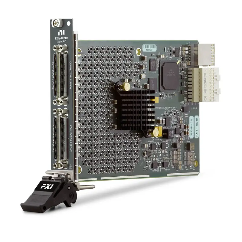
Product Introduction
Земля NI PXIe-7821R is a PXI Express digital reconfigurable I/O module designed for applications requiring high-speed digital I/O, deterministic hardware timing, custom digital protocols, sensor simulation, hardware-in-the-loop (HIL) testing, and automated electronic test.
The PXIe-7821R combines 128 bidirectional digital I/O channels с программируемым пользователем Xilinx Kintex-7 160T FPGA и 512 MB of onboard DRAM. Its FPGA-based architecture allows engineers to implement application-specific timing, triggering, signal generation, protocol handling, and decision-making directly in hardware.
With support for digital clock rates up to 80 MHz and software-selectable logic levels including 1.2 V, 1.5 V, 1.8 V, 2.5 V, and 3.3 V, the PXIe-7821R provides a flexible platform for interfacing with a wide range of digital electronic devices.
Product Overview
Земля National Instruments PXIe-7821R belongs to the NI R Series family of FPGA-based reconfigurable I/O devices.
Unlike conventional fixed-function digital I/O modules, the PXIe-7821R provides a user-programmable FPGA that allows the behavior of the digital channels to be customized for a specific application.
Individual digital lines can be configured through FPGA logic for functions such as:
- Digital inputs
- Digital outputs
- Counter/timers
- Генерация ШИМ
- Encoder inputs
- Пользовательские цифровые протоколы
- Hardware triggering
- Pattern generation
- Sensor simulation
- Hardware-in-the-loop interfaces
This makes the PXIe-7821R particularly useful when standard digital I/O hardware cannot provide the required timing or protocol flexibility.
Key Features
128 Bidirectional Digital I/O Channels
The PXIe-7821R provides 128 bidirectional digital I/O channels.
The large channel count makes the module suitable for applications requiring many digital signals within a single PXI Express instrument.
Типичные применения включают:
- Digital device interfacing
- ECU testing
- Sensor simulation
- Digital pattern generation
- Protocol emulation
- Hardware-in-the-loop testing
- Production functional testing
Up to 80 MHz Digital I/O
The PXIe-7821R supports a maximum digital I/O frequency of up to 80 MHz.
This allows the module to handle high-speed digital signals while maintaining FPGA-based hardware timing.
Applications can include high-speed waveform generation, digital acquisition, protocol testing, and bit error rate testing.
Xilinx Kintex-7 160T FPGA
At the center of the PXIe-7821R is a Xilinx Kintex-7 160T FPGA.
The FPGA provides programmable hardware resources that can execute multiple digital operations in parallel with deterministic timing.
FPGA logic can be used to implement:
- Custom digital interfaces
- Hardware state machines
- Triggering logic
- Protocol encoding and decoding
- Signal generation
- Signal acquisition
- Real-time decision making
- Counter and timer functions
101,400 FPGA LUTs
The Kintex-7 160T FPGA provides 101,400 lookup tables (LUTs).
These programmable logic resources can be used to implement custom digital algorithms, communication protocols, state machines, and hardware control functions.
202,800 Flip-Flops
The PXIe-7821R FPGA provides 202,800 flip-flops.
These resources support highly parallel and deterministic digital processing architectures.
600 DSP48 Slices
The Kintex-7 160T FPGA includes 600 DSP48 slices.
Dedicated DSP resources can support arithmetic and signal-processing operations implemented directly in FPGA hardware.
11,700 kbit Block RAM
The PXIe-7821R provides approximately 11,700 kbit of embedded FPGA Block RAM.
Block RAM can be used for:
- FIFO buffers
- Lookup tables
- Temporary digital data storage
- Pattern buffers
- Protocol processing
- FPGA state information
512 MB Onboard DRAM
In addition to FPGA Block RAM, the PXIe-7821R provides 512 MB of onboard DRAM.
The larger external memory is useful for applications requiring substantial data buffering, such as:
- Long digital waveform generation
- Высокоскоростной сбор данных
- Large pattern storage
- Sensor simulation
- Регистрация данных
- Custom FPGA processing
Up to 800 MB/s DRAM Streaming
The PXIe-7821R contains one 512 MB DRAM bank with a maximum theoretical streaming bandwidth of approximately 800 MB/s.
This memory provides additional buffering capacity for applications where the FPGA’s internal Block RAM is insufficient.
Software-Selectable Logic Levels
The PXIe-7821R supports multiple digital logic levels, providing flexibility when interfacing with different electronic devices.
Supported logic levels include:
- 1.2 V
- 1.5 V
- 1.8 V
- 2.5 V
- 3.3 V
Digital I/O voltage selection is programmable per connector and defined as part of the FPGA configuration.
Four External Clock Inputs
The PXIe-7821R provides four external clock inputs.
External clocks can be used when digital I/O operations must be synchronized with external devices or custom test hardware.
FPGA Timebase Options
The FPGA supports multiple internal timebase options:
- 40 MHz
- 80 MHz
- 120 MHz
- 160 MHz
- 200 МГц
The default FPGA timebase is 40 MHz.
Deterministic Hardware Timing
Because timing and decision logic execute directly in the FPGA, the PXIe-7821R can provide deterministic hardware-timed behavior.
This is particularly useful for applications where operating-system or software latency would be unacceptable.
Custom Digital Protocols
The user-programmable FPGA allows engineers to implement specialized communication protocols directly in hardware.
Custom FPGA logic can provide:
- Protocol state machines
- Custom packet formats
- Bit-level timing
- Encoding and decoding
- Hardware handshaking
- Error detection
- Deterministic responses
Peer-to-Peer Streaming
The PXIe-7821R supports PXI Express peer-to-peer streaming, allowing compatible PXI Express modules to transfer data directly between instruments.
A typical architecture can be:
PXI Measurement Module → PXIe-7821R FPGA → PXI Output Module
This can reduce host processor involvement in suitable high-speed test architectures.
16 DMA Channels
The PXIe-7821R provides 16 DMA channels for transferring data between FPGA resources and the host system.
DMA-based transfer is useful for moving large amounts of digital data while reducing CPU overhead.
PCI Express x4 Bus Interface
The PXIe-7821R uses an x4 PCI Express bus interface for communication with the host system.
The architecture supports DMA, interrupts, and programmed I/O data transfers.
Technical Specifications
| Параметр | Спецификация |
|---|---|
| Product Type | PXI Digital Reconfigurable I/O Module |
| Модель | NI PXIe-7821 / PXIe-7821R |
| Part Number | 783485-01 |
| Platform | PXI Express |
| Digital I/O Channels | 128 Bidirectional Channels |
| Maximum Digital I/O Frequency | 80 MHz |
| ФПГА | Xilinx Kintex-7 160T |
| FPGA LUTs | 101,400 |
| FPGA Flip-Flops | 202,800 |
| DSP48 Slices | 600 |
| Embedded Block RAM | 11,700 kbit |
| Onboard DRAM | 512 MB |
| DRAM Banks | 1 |
| Maximum Theoretical DRAM Streaming Rate | 800 MB/s |
| Digital Logic Levels | 1.2 V, 1.5 V, 1.8 V, 2.5 V, 3.3 V |
| External Clock Inputs | 4 |
| FPGA Timebases | 40, 80, 120, 160 and 200 MHz |
| Default FPGA Timebase | 40 MHz |
| DMA Channels | 16 |
| Шинный интерфейс | x4 PCI Express |
| Peer-to-Peer Streaming | Supported |
| FPGA Programmable | Да |
| Primary Applications | HIL Test, Sensor Simulation, Digital Protocols, Waveform Generation and Automated Test |
What Is Reconfigurable Digital I/O?
A conventional digital I/O module generally provides a predefined set of timing and acquisition functions.
A reconfigurable I/O module such as the PXIe-7821R adds a user-programmable FPGA between the digital I/O hardware and the host computer.
A simplified architecture is:
Digital DUT → 128 DIO → Kintex-7 FPGA → DRAM / DMA → PXI Express Controller
This architecture allows digital signals to be processed directly in hardware before data is transferred to the host.
How Does the PXIe-7821R Work?
The PXIe-7821R combines programmable digital I/O with FPGA-based hardware processing.
Instead of requiring the host processor to respond to every digital event, the FPGA can execute the required logic directly on the module.
Например:
Digital Input → FPGA Condition Detection → Hardware Decision → Digital Output
This architecture enables deterministic responses and highly customized digital behavior.
Digital Input Applications
Any of the 128 bidirectional digital channels can be configured for input functionality according to the FPGA application.
Digital input applications can include:
- Logic-state monitoring
- Digital pattern acquisition
- Encoder input
- Protocol decoding
- Event detection
- Hardware triggering
- Device status monitoring
Digital Output Applications
Digital lines can also be configured as outputs for generating deterministic digital signals.
Applications can include:
- Цифровое формирование сигналов
- Device control
- Sensor simulation
- Генерация ШИМ
- Protocol emulation
- Digital pattern generation
- Trigger generation
Counter and Timer Applications
Because counter and timer functions can be implemented in FPGA logic, engineers can create application-specific timing architectures rather than relying only on a fixed number of hardware counters.
Possible functions include:
- Подсчет событий
- Frequency measurement
- Period measurement
- Pulse-width measurement
- Генерация импульсов
- Custom timing sequences
PWM Generation
The PXIe-7821R can implement PWM generation through custom FPGA logic.
PWM applications can include:
- Motor control signal simulation
- ECU testing
- Industrial control simulation
- Electronic device stimulation
- Custom pulse generation
Encoder Simulation and Measurement
FPGA-based digital I/O can be used to acquire or simulate encoder signals.
This can be useful in HIL systems for testing:
- Motor controllers
- Motion-control systems
- Automotive ECUs
- Industrial controllers
- Встроенные системы управления
Sensor Simulation
NI identifies sensor simulation as one of the primary application areas for the PXIe-7821R.
The module can generate deterministic digital signals that reproduce the behavior of compatible sensors and interfaces.
A typical HIL architecture can be:
Test Model → PXIe-7821R FPGA → Simulated Digital Sensor Signals → ECU
Hardware-in-the-Loop Testing
The PXIe-7821R is well suited for hardware-in-the-loop (HIL) testing because FPGA logic can provide deterministic digital stimulus and response.
A typical HIL test system can use the module for:
- Digital sensor simulation
- Actuator signal monitoring
- PWM generation and measurement
- Encoder simulation
- Custom protocol communication
- Fault simulation
- Детерминированное срабатывание
Bit Error Rate Testing
The PXIe-7821R can be used in digital bit error rate test applications requiring customized pattern generation and acquisition.
FPGA logic can generate a known digital sequence, acquire the returned data, compare transmitted and received patterns, and count detected errors.
A simplified architecture is:
FPGA Pattern Generator → DUT → FPGA Pattern Comparison → Error Count
High-Speed Waveform Generation
The combination of 128 digital channels, FPGA timing, and onboard DRAM makes the PXIe-7821R suitable for customized high-speed digital waveform generation.
The 512 MB DRAM can store large digital patterns that are streamed through FPGA logic to the digital outputs.
Custom Protocol Implementation
The PXIe-7821R can implement specialized or proprietary digital communication protocols.
This is useful when the DUT uses a protocol that cannot be adequately tested using a conventional digital I/O instrument.
FPGA logic can control:
- Clock generation
- Data framing
- Handshaking
- Protocol state machines
- Bit timing
- Error handling
- Response generation
Real-Time Hardware Decision Making
One of the major advantages of the PXIe-7821R is the ability to execute custom decision logic directly on the FPGA.
Например:
Input Event Detected → FPGA Evaluates Condition → Output Response Generated
This avoids the variable latency associated with routing every event through the host operating system.
Onboard DRAM for Large Digital Patterns
The 512 MB onboard DRAM provides substantially more storage than the FPGA’s embedded Block RAM.
This memory can be useful for:
- Large waveform buffers
- Long digital test patterns
- Sensor simulation data
- Acquired digital data
- Intermediate FPGA processing data
PXIe-7821R vs PXIe-7820R
The PXIe-7821R and PXIe-7820R are closely related R Series digital reconfigurable I/O modules. The PXIe-7821R adds onboard DRAM, making it more suitable for applications requiring large data buffers or long digital patterns.
| Функция | PXIe-7821R | PXIe-7820R |
|---|---|---|
| ФПГА | Кинтекс-7 160Т | Кинтекс-7 160Т |
| Цифровой ввод-вывод | 128 | 128 |
| Maximum DIO Rate | 80 MHz | 80 MHz |
| Onboard DRAM | 512 MB | No |
| Primary Advantage | Large Data and Pattern Buffering | Applications Not Requiring DRAM |
PXIe-7821R vs PXIe-7822R
The PXIe-7822R provides a larger FPGA than the PXIe-7821R while retaining onboard DRAM, making it suitable for applications requiring more FPGA logic resources.
| Функция | PXIe-7821R | PXIe-7822R |
|---|---|---|
| ФПГА | Кинтекс-7 160Т | Кintex-7 325T |
| Onboard DRAM | 512 MB | 512 MB |
| DRAM Bandwidth | 800 MB/s | 800 MB/s |
| Best Application | Moderate FPGA Resource Requirements | More Complex FPGA Applications |
PXIe-7821R vs Conventional Digital I/O
| Функция | PXIe-7821R | Conventional Digital I/O |
|---|---|---|
| Digital Channels | 128 Bidirectional | Device Dependent |
| ФПГА | User Programmable | Usually No |
| Custom Protocols | Да | Ограниченный |
| Hardware Decision Logic | Customizable | Fixed Function |
| Deterministic Timing | FPGA Based | Device Dependent |
| Onboard DRAM | 512 MB | Device Dependent |
| Best Application | Custom High-Speed Digital Test | Standard Digital I/O |
PXIe-7821R in a Complete PXI System
The PXIe-7821R can provide FPGA-based digital I/O within a complete PXI system.
A typical system can include:
- PXI Шасси
- PXI Контроллер
- PXIe-7821R Digital Reconfigurable I/O Module
- Модули PXI
- PXI data acquisition modules
- PXI oscilloscopes and digitizers
- PXI switching modules
- PXI Source Measure Units
- PXI timing and synchronization hardware
This modular architecture allows digital FPGA functions to be combined with analog measurement, switching, RF, power, and other test capabilities.
Software and FPGA Programming
The PXIe-7821R is designed for user-programmable FPGA applications using compatible NI FPGA development software.
With LabVIEW FPGA, engineers can define custom hardware functionality including:
- Digital input and output
- Counter/timers
- PWM
- Интерфейсы энкодера
- Пользовательские протоколы связи
- Hardware triggering
- Data buffering
- Real-time decision making
Software compatibility should be verified for the specific development environment and system configuration.
Compatible Accessories
NI provides accessories for connecting the PXIe-7821R to external digital hardware.
Compatible accessories can include:
- SHC68-C68-RDIO2 shielded R Series high-speed digital cable
- SCB-68 HSDIO shielded 68-pin connector block
- Compatible digital test fixtures and breakout hardware
The appropriate cable and terminal hardware should be selected according to the DUT interface and system wiring requirements.
How to Choose a Digital Reconfigurable I/O Module
Before selecting the PXIe-7821R, engineers should evaluate:
- Required number of digital channels
- Maximum digital signal frequency
- Required logic voltage levels
- FPGA resource requirements
- Onboard memory requirements
- External clock requirements
- Custom protocol requirements
- HIL test requirements
- Peer-to-peer streaming requirements
- PXI Express chassis compatibility
- FPGA software requirements
- Cable and connector requirements
Industries
- Automotive Electronics
- Hardware-in-the-Loop Test
- Automated Test Equipment
- Аэрокосмическая и оборонная промышленность
- Electronic Manufacturing
- Тестирование полупроводников
- Промышленная автоматизация
- Embedded Systems
- Research and Development
Applications
Hardware-in-the-Loop Testing
The PXIe-7821R can provide deterministic digital stimulus, acquisition, protocol handling, and sensor simulation for HIL test systems.
Sensor Simulation
FPGA-programmable digital channels can generate deterministic signals that simulate compatible digital sensors and interfaces.
High-Speed Digital Waveform Generation
The combination of 128 digital channels, 80 MHz operation, FPGA timing, and 512 MB DRAM supports custom high-speed digital waveform generation.
Bit Error Rate Testing
FPGA logic can generate digital patterns, acquire returned data, compare the patterns, and calculate digital errors for customized BER test applications.
Custom Digital Protocols
The Kintex-7 FPGA can implement proprietary or application-specific digital communication protocols with deterministic hardware timing.
Automated Production Test
The PXIe-7821R can be integrated into automated functional test systems requiring high-density programmable digital I/O.
Recommended Related Products
| NI PXIe-7821R | 128-channel digital reconfigurable I/O module with Kintex-7 160T FPGA and 512 MB onboard DRAM. |
| NI PXIe-7820R | 128-channel R Series digital reconfigurable I/O module using a Kintex-7 160T FPGA for applications that do not require onboard DRAM. |
| NI PXIe-7822R | Digital reconfigurable I/O module with a larger Kintex-7 325T FPGA and 512 MB DRAM for applications requiring additional FPGA resources. |
| NI PXI Modules | PXI instrumentation for digital I/O, data acquisition, FPGA processing, switching, signal generation, and automated test. |
Why Choose NI PXIe-7821R?
- 128 bidirectional digital I/O channels
- Up to 80 MHz digital I/O
- Xilinx Kintex-7 160T FPGA
- 101,400 FPGA LUTs
- 202,800 flip-flops
- 600 DSP48 slices
- 11,700 kbit embedded Block RAM
- 512 MB onboard DRAM
- Up to 800 MB/s theoretical DRAM streaming
- 1.2 V to 3.3 V selectable logic levels
- Four external clock inputs
- 16 DMA channels
- Peer-to-peer streaming support
- Custom hardware-timed decision making
- Suitable for HIL and sensor simulation
- Suitable for custom digital protocols
Frequently Asked Questions
What is the NI PXIe-7821R?
The NI PXIe-7821R is a PXI Express digital reconfigurable I/O module featuring 128 bidirectional digital channels, a Xilinx Kintex-7 160T FPGA, and 512 MB of onboard DRAM.
What is the part number of the PXIe-7821R?
The NI ordering part number for the PXIe-7821R is 783485-01.
How many digital channels does the PXIe-7821R have?
The PXIe-7821R provides 128 bidirectional digital I/O channels.
What is the maximum clock rate of the PXIe-7821R?
The digital I/O supports a maximum clock rate of up to 80 MHz.
What FPGA does the PXIe-7821R use?
The PXIe-7821R uses a Xilinx Kintex-7 160T FPGA.
How much DRAM does the PXIe-7821R have?
The module provides 512 MB of onboard DRAM in one memory bank.
What is the DRAM bandwidth of the PXIe-7821R?
NI specifies a maximum theoretical DRAM streaming data rate of approximately 800 MB/s.
What digital logic levels does the PXIe-7821R support?
Supported digital logic levels include 1.2 V, 1.5 V, 1.8 V, 2.5 V, and 3.3 V.
Can the PXIe-7821R generate PWM signals?
Yes. PWM generation can be implemented using custom FPGA logic.
Can the PXIe-7821R be used as a counter or timer?
Yes. Digital lines and FPGA resources can be configured to implement counter and timer functionality.
Can the PXIe-7821R read encoder signals?
Yes. NI identifies encoder input as one of the configurable digital I/O functions supported through FPGA programming.
Can the PXIe-7821R implement custom communication protocols?
Yes. The user-programmable FPGA allows specialized digital communication protocols and hardware state machines to be implemented directly on the module.
Can the PXIe-7821R be used for HIL testing?
Yes. HIL testing is one of the primary applications identified by NI for the PXIe-7821R.
Can the PXIe-7821R be used for sensor simulation?
Yes. Its deterministic FPGA-based digital I/O makes the module suitable for compatible digital sensor simulation applications.
Does the PXIe-7821R support peer-to-peer streaming?
Yes. The module supports peer-to-peer streaming for direct data transfer between compatible PXI Express modules.
What is the difference between PXIe-7820R and PXIe-7821R?
Both use the Kintex-7 160T FPGA and provide 128 digital I/O channels. A major advantage of the PXIe-7821R is its 512 MB onboard DRAM, making it better suited for large waveform, pattern, and data-buffering applications.
What is the difference between PXIe-7821R and PXIe-7822R?
Both provide onboard DRAM, but the PXIe-7822R uses a larger Kintex-7 325T FPGA. The PXIe-7822R is therefore more appropriate when the FPGA application requires substantially more programmable logic resources.
What should I check before purchasing a PXIe-7821R?
Before purchasing the PXIe-7821R, verify the required digital channel count, clock rate, logic voltage, FPGA resources, onboard DRAM requirements, external clock requirements, connector and cable requirements, PXI Express chassis compatibility, FPGA software compatibility, and exact NI ordering part number.
Заключение
Земля NI PXIe-7821R Digital Reconfigurable I/O Module combines 128 bidirectional digital I/O channels, an 80 MHz maximum digital clock rate, a Xilinx Kintex-7 160T FPGA, and 512 MB of onboard DRAM in a PXI Express platform. Its programmable FPGA architecture, selectable digital logic levels, deterministic hardware timing, peer-to-peer streaming, and large onboard memory make it well suited for hardware-in-the-loop testing, sensor simulation, custom digital protocols, high-speed waveform generation, bit error rate testing, and automated electronic test systems.















