







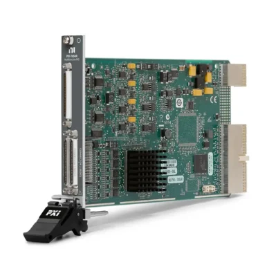
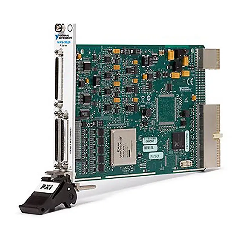
PXI-7852 Virtex-5 LX50 FPGA Multifunction RIO Module
Земля PXI-7852 is a multifunction reconfigurable I/O module featuring a user-programmable Virtex-5 LX50 FPGA. It combines analog input, analog output and digital I/O capabilities for deterministic test, measurement and control applications.
With 8 analog inputs, 8 analog outputs, 96 bidirectional digital I/O lines and analog input sampling rates up to 750 kS/s per channel, the PXI-7852 is suitable for hardware-in-the-loop testing, sensor simulation, custom protocol development and high-speed control.
Key Features of the PXI-7852
- Virtex-5 LX50 user-programmable FPGA
- 8 simultaneously sampled analog input channels
- 16-bit analog input resolution
- 750 kS/s maximum sampling rate per analog input
- 8 аналоговых выходных каналов
- 16-bit analog output resolution
- Up to 1 MS/s analog output update rate
- 96 bidirectional digital I/O lines
- 40 MHz maximum digital clock rate
- 3.3 V and 5 V digital logic compatibility
- Independent channel timing and triggering
- Support for multirate sampling
- PXI Hybrid bus connector
PXI-7852 Technical Specifications
| Product Model | PXI-7852 |
|---|---|
| Part Number | 780340-01 |
| Product Type | PXI Multifunction Reconfigurable I/O Module |
| ФПГА | Virtex-5 LX50 |
| Onboard DRAM | Ничего |
| Analog Inputs | 8 |
| Analog Input Resolution | 16 bit |
| Maximum Analog Input Rate | 750 kS/s per channel |
| Analog Input Ranges | ±1 V, ±2 V, ±5 V and ±10 V |
| Input Modes | Differential, RSE and NRSE |
| Analog Outputs | 8 |
| Analog Output Resolution | 16 bit |
| Maximum Analog Output Rate | 1 Мвыб/с на канал |
| Analog Output Range | ±10 V |
| Цифровой ввод-вывод | 96 bidirectional lines |
| Maximum Digital Clock Rate | 40 MHz |
| Digital Logic Levels | 3.3 V and 5 V |
| Bus Connector | PXI Hybrid |
| Data Transfer | DMA, interrupts and programmed I/O |
PXI-7852 Part Number and Accessories
| Item | Part Number | Описание |
|---|---|---|
| PXI-7852 | 780340-01 | Virtex-5 LX50 FPGA multifunction RIO module |
| SCB-68A | 782536-01 | Shielded 68-pin screw-terminal connector block |
| SHC68-68-RMIO | 189588-01 | 1 m shielded cable for multifunction RIO connections |
| SHC68-68-RDIO | 191667-01 | 1 m shielded cable for reconfigurable digital I/O |
| SHC68-NT-S | 189041-02 | 2 m shielded cable with unterminated leads |
Required cables and terminal blocks depend on the connector and signal groups used in the application. Verify pinout and accessory compatibility before ordering.
Virtex-5 LX50 FPGA Processing
The onboard Virtex-5 LX50 FPGA provides direct hardware-level control over analog and digital I/O. Engineers can create custom timing, triggering, signal processing and communication functions that operate independently of the host operating system.
This architecture provides deterministic execution and low-latency response for applications that cannot be handled effectively by conventional software-timed data acquisition hardware.
Simultaneous Analog Input Acquisition
The PXI-7852 provides eight 16-bit analog input channels. Each channel has a dedicated successive-approximation ADC, allowing all channels to acquire signals simultaneously at rates up to 750 kS/s per channel.
Dedicated ADCs also support independent timing and triggering, enabling multirate acquisition and application-specific sampling behavior.
Programmable Analog Input Ranges
Selectable input ranges of ±1 V, ±2 V, ±5 V and ±10 V allow the module to measure signals with different voltage levels. Choosing the smallest suitable range can improve the effective measurement resolution.
The PXI-7852 supports differential, referenced single-ended and nonreferenced single-ended input configurations. The appropriate mode depends on signal grounding, cable length and noise conditions.
FPGA-Timed Analog Output
Eight 16-bit analog output channels provide waveform generation and control outputs with update rates up to 1 Мвыб/с на канал. FPGA-based timing allows the outputs to respond deterministically to analog measurements or digital events.
Typical uses include actuator control, sensor simulation, stimulus generation and closed-loop test systems.
96 Bidirectional Digital I/O Lines
The PXI-7852 includes 96 bidirectional digital I/O lines. Each line can be configured through the FPGA application for input, output, timing, triggering or custom protocol functions.
The digital channels support 3.3 V and 5 V logic and operate with clock rates up to 40 MHz. This large channel count is useful for interfacing with embedded devices, digital control systems and custom test fixtures.
Independent Timing and Triggering
Timing and trigger logic can be implemented directly in the FPGA rather than relying on fixed hardware functions. Analog inputs, analog outputs and digital lines can operate at different rates while remaining synchronized within the same FPGA design.
Users can implement custom trigger qualification, digital handshaking, event sequencing, pulse generation and precise closed-loop responses.
Типичные применения
- Симуляция с аппаратным входом
- Custom protocol communication
- Sensor and actuator simulation
- High-speed closed-loop control
- Automotive electronic control unit testing
- Power electronics validation
- Motor control development
- Обработка сигналов на основе ПЛИС
- Automated production testing
- Electronic device validation
LabVIEW FPGA Programming
The PXI-7852 can be customized using the LabVIEW FPGA Module and compatible NI-RIO software. Developers can build application-specific FPGA personalities without designing separate FPGA hardware.
After compilation, the FPGA application executes directly on the module, providing deterministic timing and control without depending on host-computer response times.
PXI Chassis Integration
The PXI-7852 uses a PXI Hybrid connector and requires a compatible PXI or PXI Express hybrid chassis slot. Before installation, verify the chassis slot type, controller compatibility, cooling capacity and supported software environment.
Explore additional hardware in the NI PXI Modules category when configuring a complete PXI test system.
Connectivity and Signal Wiring
Compatible SHC68 cables and SCB-68 series connector blocks provide access to the analog and digital signals. Use the correct pinout label for the PXI-7852 because terminal assignments can differ between NI R Series models.
Proper shielding, grounding and cable routing are important when combining low-level analog measurements with high-speed digital signals.
Troubleshooting the PXI-7852
The module is not detected by the system
Confirm that the PXI-7852 is installed in a compatible PXI Hybrid slot. Check the chassis controller, PXI Platform Services and NI-RIO driver installation.
The FPGA bitfile cannot be downloaded
Verify that the bitfile was compiled specifically for the PXI-7852 and that the installed LabVIEW FPGA and NI-RIO versions support the module.
Analog input measurements are noisy
Check grounding, shielding, input mode and cable routing. Select the smallest appropriate input range and keep sensitive analog wiring away from power cables and high-speed digital signals.
Digital signals are not operating correctly
Confirm the selected line direction, terminal assignment and external ground connection. Make sure the connected device uses a compatible 3.3 V or 5 V logic level.
The system reports a connector or pinout mismatch
Check that the cable, terminal block and PXI-7852 pinout label are correct. R Series modules may use different signal assignments even when they use similar 68-pin connectors.
PXI-7852 Comparison
| Модель | ФПГА | Analog Input Rate | Цифровой ввод-вывод | Конфигурация |
|---|---|---|---|---|
| PXI-7852 | Virtex-5 LX50 | 750 kS/s | 96 | 8 AI and 8 AO |
| PXI-7851 | Virtex-5 LX30 | 750 kS/s | 96 | 8 AI and 8 AO |
| ПХИ-7842 | Virtex-5 LX50 | 200 kS/s | 96 | 8 AI and 8 AO |
| ПХИ-7841 | Virtex-5 LX30 | 200 kS/s | 96 | 8 AI and 8 AO |
Recommended Related Products
- PXI-7851 – 750 kS/s multifunction RIO module with a Virtex-5 LX30 FPGA
- ПХИ-7842 – Virtex-5 LX50 module with a 200 kS/s analog input rate
- ПХИ-7841 – 200 kS/s multifunction RIO module with a Virtex-5 LX30 FPGA
- PXIe-7857 – newer PXI Express RIO module with a Kintex-7 FPGA and onboard DRAM
- PXIe-7858 – high-capacity Kintex-7 325T FPGA module with 512 MB DRAM
Selecting the PXI-7852
Choose the PXI-7852 when your system requires 750 kS/s simultaneous analog acquisition, eight analog outputs, 96 digital I/O lines and a Virtex-5 LX50 FPGA in a PXI Hybrid platform.
For a smaller FPGA design with the same principal I/O configuration, consider the PXI-7851. For new PXI Express systems requiring more FPGA resources and onboard memory, consider the PXIe-7857 or PXIe-7858.
PXI-7852 vs PXI-7851
The PXI-7852 and PXI-7851 both provide eight analog inputs, eight analog outputs, 96 digital I/O lines and analog input sampling rates up to 750 kS/s per channel.
The main difference is FPGA capacity. The PXI-7852 uses a Virtex-5 LX50 FPGA, while the PXI-7851 uses a Virtex-5 LX30 FPGA. The PXI-7852 is better suited to applications requiring more complex FPGA logic or additional parallel processing.
Why Choose the PXI-7852?
- Simultaneous 16-bit analog input acquisition
- 750 kS/s sampling on every analog input channel
- Eight FPGA-timed analog outputs
- 96 configurable digital I/O lines
- Virtex-5 LX50 FPGA for custom onboard processing
- Independent channel timing and triggering
- Suitable for existing PXI Hybrid test systems
Frequently Asked Questions
What is the PXI-7852 used for?
The PXI-7852 is used for FPGA-based data acquisition, hardware-in-the-loop testing, custom protocol communication, sensor simulation and deterministic control.
Which FPGA does the PXI-7852 use?
It uses a user-programmable Virtex-5 LX50 FPGA.
How many analog channels does the PXI-7852 provide?
The module provides eight 16-bit analog inputs and eight 16-bit analog outputs.
What is the maximum analog input sampling rate?
Each analog input channel can acquire signals at rates up to 750 kS/s.
How many digital I/O lines are available?
The PXI-7852 provides 96 bidirectional digital I/O lines with a maximum clock rate of 40 MHz.
Does the PXI-7852 include onboard DRAM?
No. The PXI-7852 does not include onboard DRAM.
Can the PXI-7852 operate independently?
No. It must be installed in a compatible PXI chassis and used with an appropriate controller, driver and FPGA application.
What is the PXI-7852 part number?
The standard NI part number for the PXI-7852 is 780340-01.
Request a Quote for the PXI-7852
Contact us for current availability, lead time and project pricing for the PXI-7852 Multifunction Reconfigurable I/O Module. We can also help confirm compatible PXI chassis, cables, connector blocks and related R Series modules for your system.















