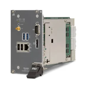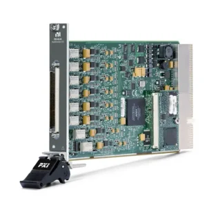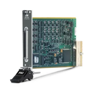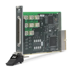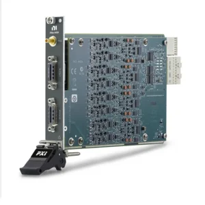


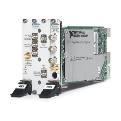
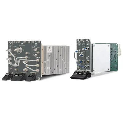
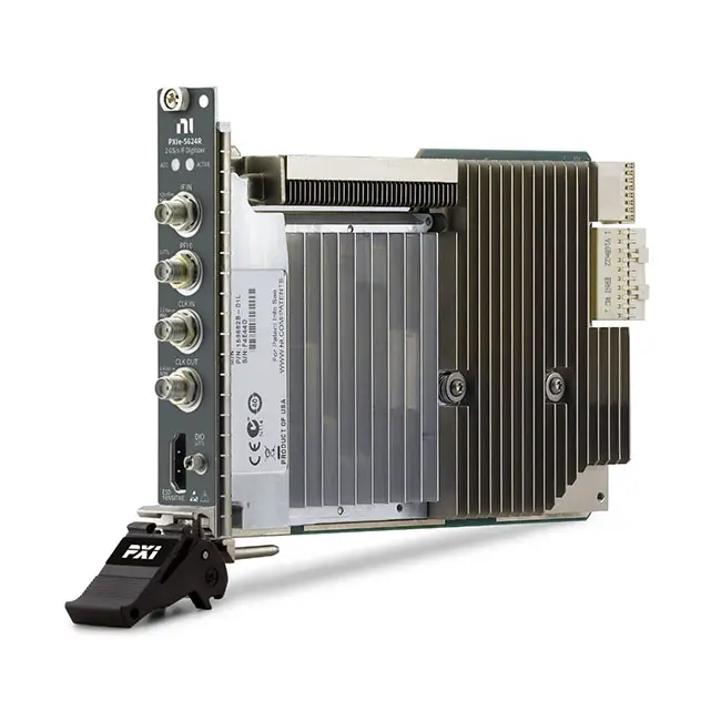
PXIe-5624 2 GS/s 12-Bit PXI Express IF Digitizer
Земля NI PXIe-5624, also identified in NI documentation as the PXIe-5624R, is a software-designed PXI Express intermediate-frequency digitizer with a user-programmable FPGA. It provides one 12-bit input channel, a 2 GS/s sampling rate and a typical input-frequency range from 5 MHz to 2 GHz.
The PXIe-5624 is optimized for superheterodyne receiver architectures. Its onboard digital downconverter converts wideband IF signals into real or complex I/Q data, allowing the module to operate as a stand-alone IF digitizer or as part of a modular PXI vector signal analyzer.
Key Features of the PXIe-5624
- Single-channel PXI Express IF digitizer
- 12-bit analog-to-digital converter resolution
- 2 GS/s digitizer-mode sampling rate
- Typical input-frequency range from 5 MHz to 2 GHz
- Up to 800 MHz equalized acquisition bandwidth
- 400 MHz and 800 MHz acquisition FPGA images
- Onboard digital downconversion
- Real and complex I/Q data generation
- User-programmable Xilinx Kintex-7 FPGA
- Frequency shifting, decimation and digital equalization
- Onboard calibration processing in DDC mode
- 2 GB onboard DRAM
- 2 MB onboard SRAM
- 32 DMA channels
- PXI Express Gen 2 x8 bus interface
- NI peer-to-peer streaming support
- Up to 3.2 GB/s peer-to-peer streaming capability
- 50 Ω AC-coupled IF input
- 20 dBm absolute maximum continuous-wave input power
- Clock input and output connectors
- Bidirectional programmable-function interface
- 12 bidirectional auxiliary digital I/O channels
- Internal, external and PXIe_CLK100 clocking options
- LabVIEW Instrument Design Libraries support
PXIe-5624 Technical Specifications
| Product Model | PXIe-5624 / PXIe-5624R |
|---|---|
| Part Number | 783132-01 |
| Product Type | PXI Express IF digitizer with user-programmable FPGA |
| Number of IF Input Channels | 1 |
| ADC Resolution | 12 bits |
| Digitizer-Mode Sample Rate | 2 GS/s |
| Typical Input-Frequency Range | 5 MHz to 2 GHz |
| Equalized Bandwidth | Up to 400 MHz or 800 MHz, depending on the FPGA image |
| 400 MHz FPGA Image Bandwidth Range | 95 Hz to 400 MHz |
| 800 MHz FPGA Image Bandwidth | 800 MHz |
| Bandwidth Resolution | 3.56 µHz with the 400 MHz acquisition FPGA image |
| Frequency-Shift Resolution | 7.13 µHz |
| Dither Frequency Range | 1 MHz to 50 MHz, typical |
| Full-Scale Input, Dither Off | 8 dBm nominal; approximately 1.58 Vpk-pk |
| Full-Scale Input, Dither On | 6 dBm nominal; approximately 1.26 Vpk-pk |
| Absolute Maximum IF Input Power | 20 dBm continuous-wave RMS |
| Input Impedance | 50 Ω nominal |
| Input Coupling | AC |
| Typical Average Noise Density | −149.5 dBFS/Hz in digitizer mode with dither disabled |
| Typical SFDR | −72 dBc from 50 MHz to 1.5 GHz |
| DDC Out-of-Band Suppression | Greater than 85 dB |
| DDC Frequency-Shift SFDR | −105 dBFS |
| Onboard FPGA | Xilinx Kintex-7 XC7K410T |
| FPGA Lookup Tables | 254,200 |
| FPGA Flip-Flops | 508,400 |
| FPGA DSP48 Slices | 1,540 |
| FPGA Embedded Block RAM | 28,620 kbits |
| Onboard DRAM | 2 GB |
| DRAM Theoretical Maximum Rate | 6.4 GB/s |
| Onboard SRAM | 2 MB |
| Number of DMA Channels | 32 |
| Data-Transfer Methods | DMA, interrupts and programmed I/O |
| PXI Express Interface | PXI Express Gen 2 x8 |
| Peer-to-Peer Streaming | Supported |
| IF Input Connector | SMA female |
| Clock Input Connector | SMA female |
| Clock Output Connector | SMA female |
| PFI 0 Connector | SMA female |
| Auxiliary I/O Connector | HDMI |
| Auxiliary Digital I/O | 12 bidirectional channels |
| Maximum Auxiliary I/O Toggle Rate | 10 MHz |
| Supported Reference Clocks | 10 MHz and 100 MHz |
| Supported External Sample Clocks | 2 GHz or 4 GHz |
| Calibration Interval | 1 year |
| Required Warm-Up Time | 20 minutes |
| Typical Power Consumption | 31.5 W with the 400 MHz acquisition FPGA image |
| Operating Temperature | 0°C to 55°C |
| Storage Temperature | −40°C to 71°C |
| Dimensions | 21.6 × 2.0 × 13.0 cm |
| Weight | 454 g |
| Module Format | 3U, one-slot PXI Express module |
| Primary Software | LabVIEW Instrument Design Libraries for IF Digitizers |
PXIe-5624 Part Number and Included Items
| Item | Part Number | Описание |
|---|---|---|
| PXIe-5624 | 783132-01 | 2 GS/s, 12-bit PXI Express IF digitizer with user-programmable FPGA |
| Module Documentation | Included | Safety, environmental and regulatory documentation |
The PXIe-5624 and PXIe-5624R names refer to the same reconfigurable IF-digitizer platform in NI product and specification documentation. Always verify part number 783132-01, the module label and the required software environment before ordering.
PXIe-5624 Connection Accessories
| Accessory Type | Recommended Interface | Приложение |
|---|---|---|
| IF Input Cable | 50 Ω SMA cable | Connects an IF source or RF downconverter to IF IN |
| Clock Cable | 50 Ω SMA cable | Connects CLK IN or CLK OUT to compatible timing hardware |
| Trigger Cable | SMA digital-signal cable | Connects an external trigger or FPGA-controlled event to PFI 0 |
| Auxiliary I/O Cable | Compatible HDMI cable or breakout fixture | Provides access to the 12 bidirectional digital I/O channels |
| Шасси PXI Express | Compatible chassis with a Gen 2 x8-capable peripheral slot | Provides power, cooling, timing and high-throughput data transfer |
Use precision 50 Ω cables and connectors suitable for the required frequency range. Protect IF IN from signals exceeding the specified 20 dBm continuous-wave maximum input power.
2 GS/s IF Digitizer Architecture
The PXIe-5624 digitizes the IF input at 2 GS/s with 12-bit resolution. Direct high-speed sampling allows signals in multiple Nyquist zones to be captured without requiring the IF signal to be located near DC.
The input-frequency range extends from 5 MHz to 2 GHz, making the module suitable for receiver architectures that translate RF signals to a high intermediate frequency before digitization.
5 MHz to 2 GHz Input Range
The PXIe-5624 has a typical 3 dB input-frequency range from 5 MHz to 2 GHz. This broad range supports direct acquisition of traditional IF signals and higher-frequency signals located in upper Nyquist zones.
When selecting a center frequency and measurement bandwidth, ensure that the equalized acquisition band does not cross the 1 GHz Nyquist boundary.
12-Bit Resolution
The 12-bit ADC provides 4,096 possible quantization levels. This combination of resolution and 2 GS/s sampling supports wideband measurements that require both high acquisition speed and useful dynamic range.
Typical effective number of bits is approximately 9.1 bits at 100 MHz, 9.0 bits at 410 MHz and 8.8 bits at 730 MHz under NI’s specified test conditions.
400 MHz and 800 MHz Acquisition Bandwidth
The PXIe-5624 supports different acquisition FPGA images. The 400 MHz image provides equalized bandwidth settings from approximately 95 Hz to 400 MHz, while the 800 MHz image supports as much as 800 MHz of equalized instantaneous bandwidth.
The 800 MHz mode can produce complex I/Q data at rates up to 1 GS/s. This makes the module suitable for wideband communications, radar, spectrum monitoring and advanced receiver testing.
Digitizer Mode
In digitizer mode, samples from the ADC are stored directly in onboard DRAM and transferred to the host. This mode provides access to the wideband digitized data before digital downconversion.
Data acquired in the standard digitizer-mode FPGA image is not automatically equalized or amplitude calibrated. Applications using this mode must account for the front-end response when calibrated measurements are required.
Digital Downconversion Mode
In DDC mode, digitized samples pass through FPGA signal processing before they are written to DRAM. The processing chain can shift the selected frequency band, decimate the data, apply equalization and compensate the measurement amplitude.
Digital downconversion converts a selected IF band into real or complex baseband data. This reduces the output data rate when the required signal bandwidth is smaller than the complete 2 GS/s acquisition bandwidth.
Frequency Shifting and I/Q Conversion
The onboard digital downconverter shifts the selected IF center frequency toward baseband and produces I/Q data for vector analysis. Frequency-shift resolution is 7.13 µHz.
Complex I/Q data preserves both amplitude and phase information, making it suitable for modulation analysis, EVM measurements, channel characterization and spectrum-analysis applications.
Digital Decimation
FPGA-based decimation reduces the sample rate after digital downconversion. This allows the data rate to be matched to the actual measurement bandwidth rather than continuously transferring the complete 2 GS/s stream.
Lower data rates reduce host-processing and storage requirements while preserving the required signal information within the selected measurement band.
Digital Equalization
DDC mode includes digital equalization for correcting the frequency response of the analog input path. Equalization improves amplitude flatness across the selected acquisition bandwidth.
NI specifies absolute amplitude accuracy as low as ±0.25 dB from 25 MHz to 1 GHz under the required temperature, dither, calibration and equalization conditions.
Dither Operation
Digital dither can be enabled to improve linearity and reduce deterministic quantization effects. With dither enabled, the nominal full-scale input is approximately 6 dBm or 1.26 Vpk-pk.
With dither disabled, the nominal full-scale input increases to approximately 8 dBm or 1.58 Vpk-pk. Select the dither setting according to the required linearity, signal level and dynamic-range performance.
High Dynamic-Range Measurements
The PXIe-5624 provides typical SFDR of approximately −72 dBc from 50 MHz to 1.5 GHz under the specified digitizer-mode conditions. Typical total harmonic distortion is also approximately −72 dBc across a substantial part of the input range.
In DDC mode, narrow and moderate measurement bandwidths can provide greater dynamic range because out-of-band signals and noise are suppressed before data transfer.
User-Programmable Kintex-7 FPGA
The onboard Xilinx Kintex-7 XC7K410T FPGA contains 254,200 lookup tables, 508,400 flip-flops, 1,540 DSP48 slices and 28,620 kbits of embedded block RAM.
Engineers can use the supplied acquisition FPGA images or create custom FPGA functionality with the appropriate LabVIEW FPGA and Instrument Design Libraries environment.
Custom processing can implement application-specific triggering, filtering, channelization, signal detection, data reduction and protocol logic close to the ADC.
2 GB Onboard DRAM
The PXIe-5624 contains 2 GB of onboard DRAM with a theoretical maximum data rate of 6.4 GB/s. DRAM stores acquired samples and supports high-speed data movement between the ADC, FPGA and host.
Onboard memory is especially useful for triggered acquisitions and temporary buffering when the input data rate exceeds the sustained transfer or storage rate of the host system.
PXI Express Gen 2 x8 Interface
The PXIe-5624 uses a PXI Express Gen 2 x8 bus connection. The high-throughput interface supports DMA transfers between the module and a PXI controller or external host computer.
The module provides 32 DMA channels, allowing custom FPGA designs to organize multiple independent data streams and transfer paths.
Peer-to-Peer Streaming
NI peer-to-peer streaming allows compatible PXI Express modules to exchange data directly without first routing every transfer through host memory. The PXIe-5624 supports peer-to-peer data rates up to approximately 3.2 GB/s under a suitable system configuration.
This capability is valuable when streaming wideband acquisition data to compatible FPGA coprocessors, storage modules or other PXI Express instruments for real-time processing.
IF Input Interface
IF IN uses a 50 Ω, AC-coupled SMA female connector. Input return loss is typically greater than 15 dB from 5 MHz to 2 GHz.
The absolute maximum continuous-wave input power is 20 dBm. Use external attenuation, filtering or limiting when the connected source can exceed the safe input rating.
Clock Input and Output
CLK IN can accept 10 MHz or 100 MHz reference clocks and 2 GHz or 4 GHz sample clocks. CLK OUT can export a 2 GHz sample clock or a compatible 10 MHz or 100 MHz reference.
Clock sharing enables the PXIe-5624 to operate coherently with RF downconverters, signal generators and additional digitizers.
Internal Frequency Reference
The internal frequency reference has an initial adjustment accuracy of ±0.2 ppm. Maximum temperature stability is ±2 ppm across the 0°C to 55°C operating range, with maximum aging of ±0.5 ppm per year.
For applications requiring improved long-term accuracy or phase coherence, the module can be locked to a suitable external reference or supported PXI Express backplane clock.
PFI Trigger and Control Interface
PFI 0 is a bidirectional SMA interface that can be configured by the FPGA for triggering, event output or other application-specific control functions.
The recommended digital operating range is 0 V to 3.3 V. The absolute input limits are −0.5 V to 5.5 V, and the maximum DC output drive strength is 24 mA.
12-Channel Auxiliary Digital I/O
The HDMI auxiliary connector provides 12 bidirectional, single-ended digital I/O channels. The channels can be controlled by the FPGA for triggering, synchronization, status monitoring and DUT control.
The digital lines support a maximum toggle rate of 10 MHz and use recommended logic levels from 0 V to 3.3 V. The connector also provides ground connections and a limited 5 V auxiliary supply.
Typical PXIe-5624 Applications
- Wideband IF signal acquisition
- Superheterodyne receiver testing
- PXI vector signal analyzers
- Digital communications analysis
- Radar and electronic-warfare testing
- Wideband spectrum monitoring
- Signal intelligence research
- Satellite and aerospace communications
- Wireless receiver validation
- Modulation and EVM measurements
- Real-time spectrum processing
- Custom FPGA signal processing
- Multichannel receiver systems
- High-throughput data streaming
- Research and development
Stand-Alone IF Digitizer Applications
The PXIe-5624 can directly acquire IF signals from receivers, mixers and communications subsystems. DDC mode converts the selected IF band to baseband I/Q data for software analysis.
This configuration is useful when the system already includes an external analog downconverter or when the signal of interest lies within the module’s 5 MHz to 2 GHz input range.
PXI Vector Signal Analyzer Integration
The PXIe-5624 can be combined with an RF downconverter such as the PXIe-5606 RF downconverter to form a wideband PXI vector signal analyzer.
In this architecture, the RF downconverter translates the selected RF spectrum to an intermediate frequency, while the PXIe-5624 digitizes and digitally processes the resulting IF signal.
PXIe-5668 System Integration
The PXIe-5624 is used as the IF digitizer within applicable PXIe-5668 vector signal analyzer configurations. The complete analyzer combines RF downconversion, high-speed IF acquisition and software-based vector analysis.
When used within a supported VSA system, control and measurement functions may be provided through NI-RFSA rather than direct access to the stand-alone IF-digitizer FPGA interface.
Radar and Spectrum Monitoring
The 800 MHz equalized bandwidth allows the PXIe-5624 to capture wide instantaneous frequency spans. FPGA processing can detect events, channelize spectrum or reduce the data before transferring it to the host.
Peer-to-peer streaming can route acquired data to compatible processing or storage hardware for extended-duration monitoring applications.
Digital Communications Analysis
The onboard digital downconverter generates complex I/Q samples required for vector communications measurements. Applications can analyze modulation quality, EVM, constellation behavior and spectral performance.
NI specifies nominal 64-QAM EVM performance of approximately −51.5 dB at 900 MHz and −50 dB at 1.8 GHz under the documented test conditions.
Поддержка программного обеспечения
The stand-alone PXIe-5624 is programmed with the LabVIEW Instrument Design Libraries for IF Digitizers. The software package includes example FPGA images for digitizer and digital-downconversion operation.
LabVIEW FPGA can be used to develop custom FPGA images. When the PXIe-5624 operates as part of a supported vector signal analyzer, the complete system may instead use NI-RFSA and compatible RF measurement software.
PXI Express Chassis Integration
The PXIe-5624 occupies one slot in a compatible 3U PXI Express chassis. For maximum data-transfer performance, install the module in a peripheral slot that provides the required PXI Express Gen 2 x8 connectivity.
NI requires the chassis fan speed to be set to high for warranted specifications. Slot blockers and EMC filler panels should be installed in unused positions to maintain the required airflow and reduce temperature drift.
Calibration Requirements
The standard calibration interval is one year. NI allows a two-year interval when 0.1 dB is added to the applicable one-year absolute-amplitude accuracy specifications.
A 20-minute warm-up is required after the chassis is powered and the Instrument Design Libraries software recognizes the module. Custom FPGA images must use the required calibration IP when calibrated DDC measurements are needed.
PXIe-5624 Troubleshooting
The PXIe-5624 Is Not Detected
Confirm that the module is fully installed in a compatible PXI Express slot. Check chassis power, controller communication and the installation of the LabVIEW Instrument Design Libraries for IF Digitizers.
No IF Signal Is Acquired
Verify the IF IN cable, input center frequency, bandwidth and acquisition state. Confirm that the signal level is within the module’s usable input range and that the correct FPGA image is loaded.
The Measured Amplitude Is Incorrect
Confirm that DDC mode, equalization and calibration processing are enabled when calibrated amplitude measurements are required. Digitizer-mode samples are not automatically equalized or calibrated.
The Signal Appears in the Wrong Frequency Position
Review the Nyquist zone, DDC center frequency and frequency-shift configuration. Make sure the selected equalized bandwidth does not cross the 1 GHz Nyquist boundary.
The Input Is Overloaded
Reduce the source power or install a suitable external attenuator. The absolute maximum IF input is 20 dBm CW, while the nominal full-scale input is approximately 6 dBm with dither enabled.
The FPGA Compilation Fails
Confirm that the required LabVIEW FPGA version, Xilinx compilation tools and Instrument Design Libraries are installed. Check that the custom design fits within the available FPGA logic, memory and DSP resources.
Data Streaming Stops or Overflows
Verify the PXI Express slot bandwidth, controller performance, DMA configuration and storage throughput. Reduce the acquisition bandwidth or use FPGA decimation if the host cannot sustain the requested data rate.
The Module Shuts Down During Operation
Check chassis airflow, fan settings and ambient temperature. The module can shut down if power consumption exceeds its protection threshold. Use slot blockers and allow the module to cool before restarting.
Clock Synchronization Fails
Verify that the selected reference or sample-clock frequency and power meet the CLK IN requirements. Check the SMA cable, 50 Ω termination and FPGA clock configuration.
Measurements Drift with Temperature
Set the chassis fan to high, install filler panels, allow the required 20-minute warm-up and perform self-calibration near the expected operating temperature.
PXIe-5624 Comparison with Related IF Digitizers
| Модель | Primary Configuration | Best Suited For |
|---|---|---|
| PXIe-5622 | 16-bit, 150 MS/s IF digitizer | Higher-resolution, narrower-band IF measurements |
| PXIe-5624 | 12-bit, 2 GS/s, 5 MHz to 2 GHz, FPGA processing | Wideband IF acquisition and custom real-time processing |
| PXIe-5668 | Wideband modular vector signal analyzer | Complete RF spectrum and modulation measurements |
| PXIe-5105 | General-purpose multi-channel digitizer | Time-domain acquisition requiring multiple input channels |
PXIe-5624 vs PXIe-5622
Земля PXIe-5622 provides 16-bit resolution and a lower sampling rate. It is appropriate when measurement resolution and dynamic range are more important than very wide instantaneous bandwidth.
The PXIe-5624 provides a 2 GS/s sampling rate, input frequencies up to 2 GHz, as much as 800 MHz of equalized bandwidth and a user-programmable FPGA. Choose it for wideband IF capture, high-throughput streaming and customized real-time processing.
PXIe-5624 vs PXIe-5668
The PXIe-5624 is an IF digitizer and does not provide a complete microwave RF front end by itself. The PXIe-5668 is a modular vector signal analyzer that combines RF downconversion with wideband IF digitization.
Select the PXIe-5624 when an external IF signal is already available or custom receiver integration is required. Select the PXIe-5668 when the application requires a complete RF vector signal-analysis system.
Selecting the PXIe-5624
Choose the PXIe-5624 when the application requires one 12-bit input channel, a 2 GS/s sampling rate, frequency coverage from 5 MHz to 2 GHz and as much as 800 MHz of instantaneous equalized bandwidth.
It is especially suitable when FPGA-based digital downconversion, custom real-time processing, multiple DMA streams or peer-to-peer data transfer are required.
Recommended Related Products
- PXIe-5622 16-Bit IF Digitizer
- PXIe-5606 RF Downconverter
- PXIe-5668 Vector Signal Analyzer
- PXIe-5451 Arbitrary Waveform Generator
- PXIe-5442 Waveform Generator
- PXI-5651 RF Signal Generator
- View More NI PXI and PXI Express Modules
Why Choose the PXIe-5624?
- Provides 2 GS/s, 12-bit IF signal acquisition
- Covers input frequencies from 5 MHz to 2 GHz
- Supports up to 800 MHz of equalized bandwidth
- Includes onboard real and complex digital downconversion
- Uses a user-programmable Kintex-7 FPGA
- Includes 2 GB of high-speed onboard DRAM
- Provides 32 independent DMA channels
- Supports PXI Express Gen 2 x8 data transfer
- Supports peer-to-peer streaming
- Provides external clock and trigger interfaces
- Includes 12 bidirectional auxiliary digital I/O channels
- Works as a stand-alone digitizer or VSA subsystem
Frequently Asked Questions
What Is the PXIe-5624?
The PXIe-5624 is a single-channel, 12-bit, 2 GS/s PXI Express IF digitizer with a user-programmable FPGA and onboard digital downconversion.
Is the PXIe-5624 the Same as the PXIe-5624R?
NI uses both PXIe-5624 and PXIe-5624R in its product documentation. The R designation emphasizes the module’s reconfigurable, user-programmable FPGA architecture.
What Is the PXIe-5624 Input-Frequency Range?
The typical 3 dB input-frequency range is 5 MHz to 2 GHz.
What Is the Maximum Acquisition Bandwidth?
The maximum equalized acquisition bandwidth is 800 MHz using the appropriate FPGA image. A separate FPGA image supports configurable bandwidths up to 400 MHz.
What Is the Maximum Sampling Rate?
The PXIe-5624 digitizes the IF input at 2 GS/s with 12-bit resolution.
Does the PXIe-5624 Include a Digital Downconverter?
Yes. Its FPGA can shift the selected IF band, decimate the samples, equalize the response and produce real or complex I/Q data.
How Much Onboard Memory Does It Provide?
The module includes 2 GB of DRAM and 2 MB of SRAM. The onboard DRAM has a theoretical maximum data rate of 6.4 GB/s.
Does the PXIe-5624 Support Peer-to-Peer Streaming?
Yes. It supports NI peer-to-peer streaming for direct data transfer between compatible PXI Express modules.
Can the PXIe-5624 Be Used as a Vector Signal Analyzer?
It can operate as the IF digitizer in a modular vector signal analyzer. A compatible RF downconverter is required when measuring RF signals outside the direct IF input architecture.
Which Software Controls the PXIe-5624?
Stand-alone FPGA operation uses the LabVIEW Instrument Design Libraries for IF Digitizers. A supported complete VSA configuration can use NI-RFSA and compatible RF measurement software.
What Is the PXIe-5624 Part Number?
The standard NI part number for the PXIe-5624 is 783132-01.
Request a Quote for the PXIe-5624
Contact us for current availability, lead time and project pricing for the NI PXIe-5624 2 GS/s 12-Bit PXI Express IF Digitizer. We can also help identify compatible RF downconverters, SMA cables, PXI Express chassis and related vector signal-analysis hardware.