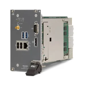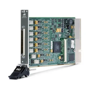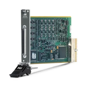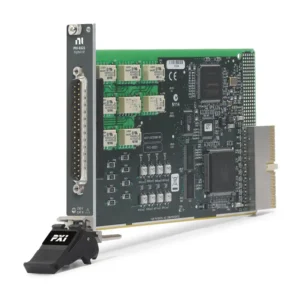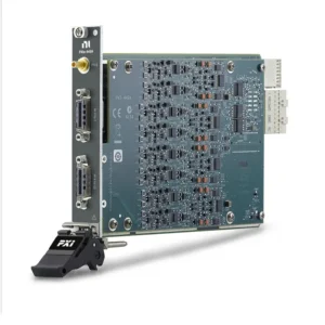


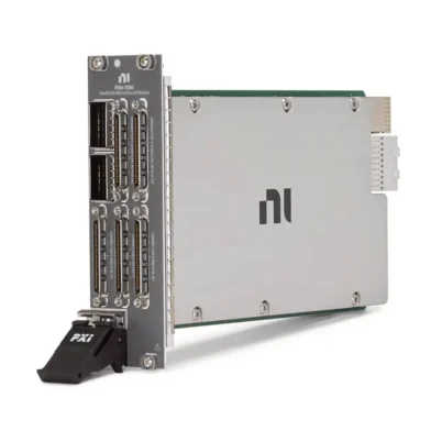
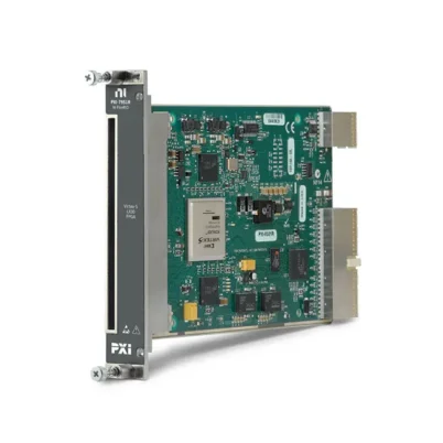
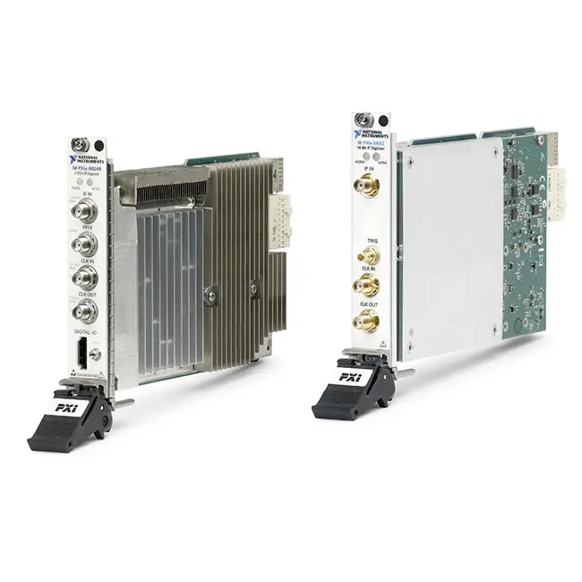
PXIe-5622 150 MS/s 16-Bit PXI IF Digitizer
Земля PXIe-5622 is a single-channel, 150 MS/s, 16-bit PXI Express intermediate-frequency digitizer designed for communications, spectrum monitoring, RF signal analysis and automated wireless testing. It provides a 50 Ω IF input, two selectable analog signal paths and onboard digital signal processing for acquiring real or complex I/Q data.
The digitizer offers a direct input path covering frequencies from 3 MHz to 250 MHz and an alias-protected 50 MHz bandpass centered at 187.5 MHz. Its onboard digital downconverter can provide as much as 60 MHz of complex flat bandwidth at a complex sample rate of 75 MS/s.
The PXIe-5622 can operate as a standalone IF digitizer or as part of an NI vector signal analyzer. It was used with compatible RF downconverters and local-oscillator modules in systems such as the PXIe-5663E, PXIe-5665 and PXIe-5667.
Key Features of the PXIe-5622
- One 50 Ω intermediate-frequency input channel
- 16-bit analog-to-digital converter resolution
- 150 MS/s maximum real-time sampling rate
- Direct-path frequency range from 3 MHz to 250 MHz
- 50 MHz bandpass centered at 187.5 MHz
- Third-Nyquist-zone bandpass acquisition
- Up to 60 MHz complex flat bandwidth
- Onboard quadrature digital downconversion
- Real and complex I/Q data-processing modes
- Programmable decimation and fractional resampling
- 48-bit numerically controlled oscillator
- 18-bit digital gain and offset adjustment
- 64 MB or 256 MB onboard memory
- Up to 100,000 waveform records
- Internal VCXO or external sample-clock operation
- PXIe backplane reference-clock synchronization
- Bidirectional PFI trigger connection
- NI-TClk multi-module synchronization
- NI-SCOPE software support
PXIe-5622 Technical Specifications
| Product Model | PXIe-5622 |
|---|---|
| Product Type | PXI Express intermediate-frequency digitizer |
| Number of Input Channels | 1 |
| Analog Input | IF IN |
| IF Input Connector | Female SMA |
| Input Impedance | 50 Ω |
| Input Coupling | AC or ground |
| ADC Resolution | 16 bits |
| Maximum Sampling Rate | 150 MS/s |
| Direct-Path Frequency Range | 3 MHz to 250 MHz, typical |
| Bandpass-Path Bandwidth | 50 MHz, centered at 187.5 MHz |
| Maximum Complex Flat Bandwidth | 60 MHz at 75 MS/s complex sample rate |
| Full-Scale Input Ranges | 0.7 Vpk-pk, 1 Vpk-pk and 1.4 Vpk-pk |
| Equivalent Input-Power Ranges | +1 dBm, +4 dBm and +7 dBm |
| Maximum Input Overload | 6.3 Vpk-pk or +20 dBm |
| Typical Input Return Loss | Better than 15 dB from 5 MHz to 300 MHz |
| Bandpass-Path Amplitude Accuracy | Less than ±0.5 dB; ±0.3 dB typical at 187.5 MHz |
| Direct-Path Amplitude Accuracy | Less than ±0.4 dB; ±0.25 dB typical at 53 MHz |
| Bandpass-Path SFDR | Better than 76.5 dBc, typical |
| Direct-Path SFDR | Better than 73 dBc, typical |
| Bandpass-Path Full-Bandwidth SNR | Greater than 66.5 dB, typical |
| Direct-Path Full-Bandwidth SNR | Greater than 67 dB, typical |
| Digital Downconverters | 1 |
| Data-Processing Modes | Real or complex I/Q |
| OSP Sample-Rate Range | 9.155 kS/s to 75 MS/s with fractional resampling |
| Maximum OSP Rate Without Fractional Resampling | 150 MS/s |
| NCO Frequency Range | 0 MHz to 75 MHz with internal sample clock |
| NCO Frequency Resolution | 533 nHz with internal sample clock |
| I/Q Phase Resolution | 0.0055° |
| Digital Gain and Offset Resolution | 18 bits |
| Onboard Memory Options | 64 MB or 256 MB |
| Real-Sample Capacity | 32 MS or 128 MS |
| Maximum Number of Records | 100,000 |
| Sample-Clock Sources | Internal VCXO or external CLK IN |
| External Sample-Clock Range | 20 MHz to 150 MHz |
| Reference-Clock Range | 1 MHz to 100 MHz in 1 MHz increments |
| Reference-Clock Sources | Front-panel CLK IN or PXIe 100 MHz backplane clock |
| PFI Trigger Connector | СМБ |
| Trigger Type | Digital |
| Minimum Trigger Pulse Width | Greater than 25 ns |
| NI-TClk Intermodule Skew | 500 ps or less, typical without manual adjustment |
| Average Skew After Manual Adjustment | 4 ps or less, typical |
| Calibration Interval | 1 year |
| Recommended Warm-Up Time | 15 minutes |
| Driver | NI-SCOPE 3.5 or later |
| Maximum Power Consumption | 32.8 W |
| Module Format | 3U, one-slot PXI Express module |
| Dimensions | 21.6 × 2.0 × 13.0 cm |
| Weight | 400 g |
| Operating Temperature | 0°C to 55°C |
| Storage Temperature | -40°C to 71°C |
PXIe-5622 Part Numbers
| Part Number | Onboard Memory | Real-Sample Capacity | Описание |
|---|---|---|---|
| 780412-01 | 64 MB | 32 megasamples | PXIe-5622 150 MS/s, 16-bit IF digitizer with standard memory |
| 780412-02 | 256 MB | 128 megasamples | PXIe-5622 150 MS/s, 16-bit IF digitizer with extended memory |
Complex I/Q data requires four bytes per sample pair, so the available complex-sample capacity is approximately half the listed real-sample capacity. Confirm the required memory version before ordering.
PXIe-5622 Connectors and Accessories
| Connection | Connector | Function |
|---|---|---|
| IF IN | Female SMA | Accepts the analog intermediate-frequency input signal |
| CLK IN | Female SMA | Accepts an external sample clock or reference clock |
| CLK OUT | Female SMA | Exports the sample clock or reference clock |
| PFI 1 | СМБ | Provides bidirectional digital triggering and event routing |
| SMA Coaxial Cable | SMA male to SMA male | Connects a downconverter IF output or clock source to the digitizer |
| 50 Ω Termination | SMA | Provides proper termination during testing and calibration |
Use high-quality 50 Ω coaxial cables and adapters with sufficient frequency range and return-loss performance. Cable loss, connector condition and impedance discontinuities can affect the amplitude and phase accuracy of the complete RF measurement system.
16-Bit IF Digitization
The PXIe-5622 uses a 16-bit analog-to-digital converter to provide greater amplitude resolution and dynamic range than conventional 8-bit oscilloscopes. This makes the module suitable for detecting relatively small signals in the presence of larger carriers or adjacent spectral components.
Actual measurement performance depends on noise, distortion, input range, clock quality and the selected analog path. The full 16-bit converter code range does not represent 16 effective noise-free bits at every input frequency.
150 MS/s Real-Time Sampling
The internal VCXO provides a 150 MS/s real-time sample clock. At this rate, the ADC Nyquist frequency is 75 MHz, but the PXIe-5622 can also acquire higher-frequency IF signals through intentional undersampling and its third-Nyquist-zone bandpass path.
The module can decimate the 150 MS/s data stream to generate lower output rates. Onboard signal processing provides alias-protected decimation when the applicable OSP mode is enabled.
Direct Input Path
The direct path provides a typical frequency range from 3 MHz to 250 MHz. It can be used for direct digitization of IF signals across several Nyquist zones.
Because signals above the first Nyquist zone fold into the sampled spectrum, engineers must understand the expected alias location and provide external filtering when unwanted frequency components could overlap the signal of interest.
Equalized measurements can provide less than ±0.6 dB amplitude flatness across the 10 MHz to 250 MHz range when referenced to 100 MHz under the specified conditions.
187.5 MHz Bandpass Path
The bandpass path provides a typical 50 MHz analog bandwidth centered at 187.5 MHz. It covers approximately 162.5 MHz to 212.5 MHz and places the signal in the ADC’s third Nyquist zone.
This path includes analog filtering to reject unwanted signals outside the selected IF band. It is particularly useful when the PXIe-5622 receives a fixed 187.5 MHz IF output from a compatible NI RF downconverter.
60 MHz Complex Analysis Bandwidth
With onboard quadrature downconversion enabled, the PXIe-5622 can provide 60 MHz of complex flat bandwidth at a 75 MS/s complex sample rate.
Complex I/Q data preserves signal amplitude and phase information, making the module suitable for modulation analysis, vector signal measurements, digital communications and spectrum processing.
Onboard Digital Downconversion
The PXIe-5622 includes one onboard digital downconverter. It can translate a selected IF signal to baseband and return complex I/Q data without requiring the host controller to process the complete 150 MS/s ADC stream.
Supported onboard processing modes include:
- Quadrature downconversion with complex I/Q output
- Real-signal downconversion with real output
- Alias-protected decimation with real output
Performing these operations onboard reduces PXI Express data-transfer requirements and allows the controller to receive only the bandwidth needed by the application.
48-Bit Numerically Controlled Oscillator
The digital downconverter uses a numerically controlled oscillator with 48-bit frequency precision. With the internal 150 MHz timebase, the NCO provides approximately 533 nHz tuning resolution across a range from 0 MHz to 75 MHz.
Fine NCO resolution allows the digital receiver to place a selected IF carrier precisely at the desired baseband frequency. I/Q phase resolution is approximately 0.0055°.
Programmable Decimation
The onboard signal-processing block supports a wide range of integer decimation values and fractional resampling from 2 through 16,384. Fractional resampling is implemented with as much as 48-bit precision.
With fractional resampling enabled, available output rates range from approximately 9.155 kS/s to 75 MS/s when using the internal clock. Without fractional resampling, operation can extend to the full 150 MS/s ADC rate.
Digital Filtering
The OSP decimation filters protect the reduced-rate data against high-frequency aliasing. The filter provides less than 0.1 dB passband ripple and more than 80 dB stopband suppression under the specified conditions.
Real output provides flat bandwidth equal to approximately 0.4 times the output sample rate. Complex output provides flat bandwidth equal to approximately 0.8 times the complex sample rate.
Setting the internal decimation rate to one and operating at 150 MS/s bypasses the onboard filtering block.
Digital Gain and Offset
The PXIe-5622 provides 18-bit digital gain and offset adjustment after digitization. Digital gain can scale the ADC data by as much as ±1.5 times its original value, while programmable offset can reposition the output data.
Digital scaling does not recover information lost through ADC clipping or improve the analog signal-to-noise ratio. The analog input range should still be selected to use the available ADC range efficiently.
Signal-to-Noise and Dynamic Range
The typical full-bandwidth signal-to-noise ratio is greater than 66.5 dB for the 187.5 MHz bandpass path and greater than 67 dB for the 53 MHz direct-path reference condition.
With digital downconversion and a reduced 4.28 MHz bandwidth, typical SNR improves to more than 71.5 dB for the bandpass path and more than 73 dB for the direct path.
Reducing the measurement bandwidth rejects out-of-band noise and improves the ability to detect low-level signals.
Spurious-Free Dynamic Range
Typical spurious-free dynamic range, including harmonics, is better than 76.5 dBc through the bandpass path and better than 73 dBc through the direct path for specified input levels.
High SFDR is valuable for harmonic, distortion, adjacent-channel and multitone measurements where small spectral components must be distinguished from digitizer-generated spurs.
Input Ranges and Protection
The PXIe-5622 provides three full-scale input ranges: 0.7 Vpk-pk, 1 Vpk-pk and 1.4 Vpk-pk. In a 50 Ω system, these correspond approximately to +1 dBm, +4 dBm and +7 dBm.
The maximum input overload is 6.3 Vpk-pk or +20 dBm. Signals above this level can damage the input circuitry. Use an external attenuator or limiter when the source can produce excessive power or transient energy.
64 MB and 256 MB Memory Options
Part number 780412-01 provides 64 MB of onboard memory, supporting approximately 32 million real samples. Part number 780412-02 provides 256 MB, supporting approximately 128 million real samples.
The extended-memory version is preferable for longer high-speed acquisitions, extensive pretrigger data and applications requiring many stored waveform records.
Multi-Record Acquisition
The digitizer can store as many as 100,000 waveform records, depending on record length and available memory. Multi-record acquisition captures only the waveform interval around each trigger and omits inactive time between events.
This capability is useful for pulsed RF, radar, burst communication and intermittent-signal applications.
Internal VCXO Clock
The onboard voltage-controlled crystal oscillator provides the internal 150 MS/s clock. Typical clock accuracy is ±5 ppm, with typical accuracy over temperature of ±12 ppm.
The VCXO can run independently or phase-lock to an external reference. Low clock phase noise helps maintain accurate phase and modulation measurements.
External Clock and Reference Input
The front-panel CLK IN connection accepts either an external sample clock or an external reference clock. External sample-clock frequencies can range from 20 MHz to 150 MHz.
Reference-clock frequencies from 1 MHz to 100 MHz are supported in 1 MHz increments. The internal VCXO can also lock to the PXIe 100 MHz backplane reference clock.
Clock Export
The CLK OUT connection can export the sample clock or reference clock to another compatible instrument. Clock sharing is useful in multi-receiver systems where several digitizers must operate from a common timing source.
Verify the required clock amplitude, impedance and cable arrangement when distributing clocks between modules.
Digital Triggering
The bidirectional PFI 1 connection accepts TTL-compatible digital triggers and can export acquisition events. Supported input destinations include start, reference, arm-reference and advance triggers.
The PFI input supports frequencies up to 20 MHz and requires a trigger pulse wider than 25 ns. As an output, it can export start, reference, end-of-record and acquisition-complete events at frequencies up to 25 MHz.
NI-TClk Synchronization
NI-TClk can align multiple supported PXI instruments through shared reference clocks and triggers. Identical PXIe-5622 modules can achieve typical intermodule skew of 500 ps or less without manual adjustment.
After manual synchronization adjustment, typical average skew can be reduced to 4 ps or less under the specified conditions. This is useful for phase-coherent multichannel receivers and synchronized RF measurement systems.
PXIe-5622 in a Vector Signal Analyzer
The PXIe-5622 is commonly used as the IF digitizer within a modular vector signal analyzer. A compatible RF downconverter converts the external RF signal to an IF accepted by the PXIe-5622.
A frequency synthesizer supplies the local-oscillator signal required by the downconverter. NI-RFSA software coordinates the downconverter, synthesizer and digitizer as one RF measurement instrument.
PXIe-5665 Integration
The PXIe-5622 was used with the PXIe-5605 wideband downconverter and PXIe-5653 synthesizer in certain PXIe-5665 Vector Signal Analyzer configurations.
Within this system, the PXIe-5622 digitizes the downconverted IF signal and provides the complex data required for spectrum, modulation and wireless measurements.
Standalone IF Digitizer Applications
The PXIe-5622 can also acquire signals directly from an external IF source without using a complete NI vector signal analyzer. The source must provide a compatible 50 Ω signal within the selected path’s frequency, power and bandwidth limits.
Standalone applications can use NI-SCOPE to configure the input path, acquire waveform records and enable onboard digital downconversion.
Communications Signal Analysis
The module can acquire digitally modulated signals and return complex I/Q data for modulation analysis. Typical applications include GSM, W-CDMA, QAM, DVB and other narrowband or wideband communication signals.
Measurement performance depends on input level, signal bandwidth, clock synchronization, selected path and the quality of the upstream RF conversion hardware.
Spectrum Monitoring
The direct and bandpass paths allow the PXIe-5622 to acquire selected IF bandwidths for spectral analysis. Onboard downconversion and decimation can reduce the data rate before transferring samples to the controller.
Long-duration or real-time spectrum-monitoring systems must account for sustained PXI Express throughput, controller performance and storage bandwidth.
Radar and Pulsed RF Testing
Deep memory, multi-record acquisition and external triggering make the PXIe-5622 suitable for pulsed RF and radar applications. Each trigger can capture a pulse or burst without recording long periods of inactive data.
Multiple synchronized modules can provide phase-related acquisition channels for research and receiver testing.
Typical PXIe-5622 Applications
- Intermediate-frequency signal digitization
- Vector signal analysis
- Wireless communication testing
- Digital modulation analysis
- Мониторинг спектра
- Radar signal acquisition
- Pulsed RF measurements
- Multitone and distortion analysis
- RF component characterization
- Automated production testing
- Phase-coherent multichannel acquisition
- Research and software-defined radio systems
- Direct IF sampling
- Onboard I/Q downconversion
NI-SCOPE Software Support
The PXIe-5622 is controlled through the NI-SCOPE instrument driver. NI-SCOPE provides functions for configuring the input path, sampling clock, triggers, waveform records and onboard signal processing.
Programming interfaces and examples are available for LabVIEW, LabWindows/CVI, Measurement Studio, Microsoft Visual C/C++ and .NET languages such as C# and Visual Basic.
NI-RFSA Integration
When the PXIe-5622 is installed as part of a supported NI vector signal analyzer, NI-RFSA coordinates the digitizer with the RF downconverter and synthesizer.
In this configuration, users generally control the complete analyzer through NI-RFSA or compatible RF measurement software instead of configuring the PXIe-5622 independently through NI-SCOPE.
Calibration
Software-controlled self-calibration corrects absolute amplitude accuracy after the module reaches a stable operating temperature. External calibration corrects absolute amplitude, relative amplitude flatness and VCXO accuracy.
The recommended external calibration interval is one year. Allow the module to warm up for at least 15 minutes and maintain adequate chassis cooling before calibration or precision measurements.
PXIe-5622 Measurement Workflow
Step 1: Select the Signal Path
Select the direct path for flexible input frequencies from 3 MHz to 250 MHz or the bandpass path for an IF centered at 187.5 MHz.
Step 2: Configure the Input Range
Choose the 0.7 V, 1 V or 1.4 V full-scale range according to the expected signal power. Prevent the source from exceeding the +20 dBm overload limit.
Step 3: Configure the Clock
Use the internal 150 MS/s VCXO, an external sample clock or a reference-locked configuration according to the synchronization requirements.
Step 4: Configure Onboard Processing
Enable the digital downconverter when complex I/Q data, real downconversion or alias-protected decimation is required. Set the NCO frequency and output rate.
Step 5: Configure Triggering
Select immediate, software or external PFI triggering and configure the required pretrigger and posttrigger sample counts.
Step 6: Acquire and Analyze Data
Acquire real or complex waveform data through NI-SCOPE or control the complete RF analyzer through NI-RFSA.
PXIe-5622 Troubleshooting
The PXIe-5622 is not detected in NI MAX
Confirm that the module is fully installed in a compatible PXI Express slot. Check chassis power, controller communication and NI-SCOPE installation, then refresh the device list in NI MAX.
The module reports a thermal-shutdown error
Stop acquisition and allow the module to cool. Set the chassis fan speed to HIGH, remove obstructed fan filters and install filler panels or slot blockers in unused slots.
No IF signal is detected
Verify the IF IN cable, source power, selected analog path and expected alias frequency. Confirm that the source is connected to IF IN rather than CLK IN.
The measured amplitude is incorrect
Check the selected input range, 50 Ω termination, cable loss, path configuration and equalization settings. Run self-calibration after the warm-up period.
The input signal is clipped
Select a larger full-scale input range or reduce the signal power with an external attenuator. Never exceed the +20 dBm maximum input overload.
The spectrum appears at the wrong frequency
Review the Nyquist-zone alias relationship, selected NCO frequency and digital downconversion settings. Higher-frequency signals can fold to a different apparent frequency after sampling.
The output sample rate is incorrect
Check the OSP decimation and fractional-resampling configuration. Non-OSP and OSP decimation cannot be enabled simultaneously.
Complex data contains I/Q errors
Verify the NCO setting, output rate, reference-clock synchronization and selected signal path. Check whether the host application interprets complex data in the correct I/Q order and numeric format.
Multiple modules are not phase aligned
Use a shared reference clock and NI-TClk synchronization. Run self-calibration and apply manual synchronization adjustment when the application requires minimum residual skew.
The 256 MB memory capacity is unavailable
Check the ordering part number. Part number 780412-01 provides 64 MB, while part number 780412-02 provides 256 MB.
PXIe-5622 Comparison with Related IF Digitizers
| Модель | Primary Configuration | Best Suited For |
|---|---|---|
| PXI-5620 | Legacy 64 MS/s, 14-bit IF digitizer | Maintaining earlier PXI RF measurement systems |
| PXI-5621 | Legacy high-resolution IF digitizer | Existing communications-analysis systems |
| PXIe-5622 | 150 MS/s, 16-bit, onboard DDC | Wideband IF and complex I/Q acquisition |
| PXI-5122 | 100 MS/s, 14-bit oscilloscope | General-purpose high-resolution time-domain measurements |
| PXIe-5606 | RF downconverter | Converting RF signals to a compatible IF |
PXIe-5622 vs General-Purpose Oscilloscope
The PXIe-5622 is optimized for IF and frequency-domain signal acquisition. It provides a 50 Ω input, bandpass sampling, digital downconversion and complex I/Q output.
A general-purpose oscilloscope normally provides multiple channels, wider voltage ranges and DC-coupled inputs for time-domain circuit measurements. Select the PXIe-5622 when IF dynamic range and complex signal analysis are more important than general oscilloscope functionality.
PXIe-5622 vs PXI-5122
Земля PXI-5122 is a two-channel, 14-bit oscilloscope with 100 MS/s sampling and general-purpose voltage inputs. The PXIe-5622 provides one 16-bit, 150 MS/s, 50 Ω IF input with onboard digital downconversion.
Choose the PXI-5122 for precision time-domain measurements requiring two channels. Choose the PXIe-5622 for communications, spectral and complex I/Q measurements.
Recommended Related Products
- PXI-5620 IF Digitizer
- PXI-5621 IF Digitizer
- PXIe-5606 RF Downconverter
- PXIe-5665 Vector Signal Analyzer
- PXI-5661 Vector Signal Analyzer
- PXI-5122 High-Resolution Oscilloscope
- PXI-5441 Arbitrary Waveform Generator
- PXIe-5673 Vector Signal Generator
- View More NI PXI and PXI Express Modules
Selecting the Right PXIe-5622 Configuration
Choose part number 780412-01 when 64 MB of memory and approximately 32 million real samples are sufficient. Select part number 780412-02 when the application requires longer acquisitions or as many as 128 million real samples.
Confirm whether the module will operate as a standalone IF digitizer or as part of a vector signal analyzer. A complete analyzer may require a specific RF downconverter, synthesizer, interconnection cable set and compatible software version.
Why Choose the PXIe-5622?
- Provides 16-bit IF digitization
- Samples at up to 150 MS/s
- Supports frequencies from 3 MHz to 250 MHz through the direct path
- Provides a filtered 50 MHz bandpass centered at 187.5 MHz
- Generates real or complex I/Q data
- Offers up to 60 MHz complex bandwidth
- Includes programmable decimation and fractional resampling
- Provides 64 MB or 256 MB memory options
- Supports shared clocks and NI-TClk synchronization
- Integrates with NI-SCOPE and compatible NI-RFSA systems
Frequently Asked Questions
What is the PXIe-5622?
The PXIe-5622 is a single-channel, 150 MS/s, 16-bit PXI Express IF digitizer for communications, spectrum and vector signal analysis.
What is the maximum sampling rate?
The maximum internal real-time sampling rate is 150 MS/s.
What is the analog input resolution?
The PXIe-5622 uses a 16-bit analog-to-digital converter.
How many input channels are provided?
The module provides one 50 Ω IF input through a female SMA connector.
What frequency range does the direct path support?
The direct path covers frequencies from 3 MHz to 250 MHz under typical operating conditions.
What is the bandpass-path bandwidth?
The bandpass path provides 50 MHz of typical analog bandwidth centered at 187.5 MHz.
What is the maximum complex bandwidth?
The onboard digital downconverter can provide 60 MHz of complex flat bandwidth at a 75 MS/s complex output rate.
Does the PXIe-5622 support digital downconversion?
Yes. It includes one onboard DDC supporting complex I/Q downconversion, real downconversion and alias-protected decimation.
What input ranges are available?
The full-scale ranges are 0.7 Vpk-pk, 1 Vpk-pk and 1.4 Vpk-pk, corresponding to approximately +1 dBm, +4 dBm and +7 dBm in a 50 Ω system.
What is the maximum safe input level?
The maximum specified input overload is 6.3 Vpk-pk or +20 dBm.
Which memory options are available?
The PXIe-5622 is available with 64 MB or 256 MB of onboard memory.
Which software controls the PXIe-5622?
NI-SCOPE controls the module as a standalone digitizer. NI-RFSA may control it when it is installed as part of a supported vector signal analyzer.
What are the PXIe-5622 part numbers?
Part number 780412-01 provides 64 MB of memory, while part number 780412-02 provides 256 MB.
Request a Quote for the PXIe-5622
Contact us for current availability, lead time and project pricing for the PXIe-5622 150 MS/s, 16-Bit PXI IF Digitizer. Please specify the required 64 MB or 256 MB memory configuration. We can also help identify compatible SMA cables, PXI Express chassis, RF downconverters, synthesizers and related vector signal analyzer modules.