






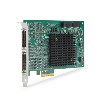
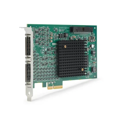
PCIe-7856 Kintex-7 Multifunction Reconfigurable I/O Device
Земля PCIe-7856 is an R Series multifunction reconfigurable I/O device for PCI Express computers. It combines eight 16-bit analog inputs, eight 16-bit analog outputs and 48 bidirectional digital I/O lines with a user-programmable Kintex-7 160T FPGA.
Each analog input has a dedicated analog-to-digital converter, enabling independent timing, multirate sampling and per-channel triggering. The analog inputs acquire at up to 1 MS/s per channel, while the analog outputs update at up to 1 MS/s per channel.
Direct FPGA control over the analog and digital I/O makes the PCIe-7856 suitable for hardware-in-the-loop testing, sensor simulation, custom protocol communication, high-speed control and other applications requiring deterministic timing.
Key Features of the PCIe-7856
- Eight 16-bit analog input channels
- Eight 16-bit analog output channels
- 48 bidirectional digital I/O channels
- 1 MS/s maximum analog input rate per channel
- 1 MS/s maximum analog output rate per channel
- Dedicated ADC for each analog input channel
- Software-selectable ±1 V, ±2 V, ±5 V and ±10 V input ranges
- ±10 V analog output range
- Kintex-7 160T user-programmable FPGA
- 101,400 FPGA lookup tables
- 600 DSP48 slices
- 11,700 kbits of embedded block RAM
- Up to 80 MHz external digital I/O
- Software-selectable digital logic families
- Sixteen DMA channels
- Eight RTSI synchronization lines
- Two 68-pin VHDCI connectors
- PCI Express x4 host interface
- LabVIEW FPGA programmability
PCIe-7856 Technical Specifications
| Product Model | PCIe-7856 |
|---|---|
| Part Number | 786455-01 |
| Product Type | R Series multifunction reconfigurable I/O device |
| ФПГА | Xilinx Kintex-7 160T |
| FPGA Flip-Flops | 202,800 |
| FPGA Lookup Tables | 101,400 |
| Embedded Block RAM | 11,700 kbits |
| DSP48 Slices | 600 |
| Onboard DRAM | 0 MB |
| Analog Input Channels | 8 |
| Analog Input Resolution | 16 bits |
| Analog Input ADC Type | Successive-approximation-register ADC, one per channel |
| Analog Input Conversion Time | 1 мкс |
| Maximum Analog Input Rate | 1 Мвыб/с на канал |
| Analog Input Modes | Differential, NRSE and RSE |
| Analog Input Ranges | ±1 V, ±2 V, ±5 V and ±10 V |
| Analog Input Coupling | DC |
| Small-Signal Input Bandwidth | 1 MHz |
| Large-Signal Input Bandwidth | 500 kHz |
| Analog Input Overvoltage Protection | ±42 V powered on; ±35 V powered off |
| Analog Output Channels | 8 |
| Analog Output Resolution | 16 bits |
| Analog Output Type | Single-ended voltage output |
| Analog Output Range | ±10 V |
| Analog Output Update Time | 1 мкс |
| Maximum Analog Output Rate | 1 Мвыб/с на канал |
| Analog Output Coupling | DC |
| Analog Output Impedance | 0.5 Ω |
| Analog Output Current Drive | ±2.5 mA |
| Analog Output Protection | Short-circuit protection to ground |
| Digital I/O Channels | 48 bidirectional channels |
| Connector 0 Digital Channels | 16 channels, up to 10 MHz |
| Connector 1 Digital Channels | 32 channels, up to 80 MHz |
| Digital Logic Families | 1.2 V, 1.5 V, 1.8 V, 2.5 V and 3.3 V |
| Default Digital Logic Level | 3.3 V |
| Maximum Digital Output Current | 4 mA source or sink per channel |
| Minimum Digital Pulse Width | 6.25 ns |
| Minimum Digital Sampling Period | 5 ns |
| External Clock Maximum Frequency | 80 MHz |
| Selectable FPGA Timebases | 40 MHz, 80 MHz, 120 MHz, 160 MHz or 200 MHz |
| Default FPGA Timebase | 40 MHz |
| Synchronization Resources | RTSI lines 0 through 7 |
| DMA Channels | 16 |
| PCI Express Interface | PCI Express x4, specification 1.0 compliant |
| Compatible Slots | PCI Express x4, x8 and x16 |
| I/O Connectors | 2 × 68-pin VHDCI |
| Form Factor | Standard-height, half-length, single-slot PCI Express card |
| Board Dimensions | 16.8 cm × 11.1 cm |
| Weight | 141.4 g |
PCIe-7856 Part Number and Accessories
| Item | Part Number | Описание |
|---|---|---|
| PCIe-7856 | 786455-01 | Kintex-7 multifunction reconfigurable I/O device with 8 AI, 8 AO and 48 DIO |
| SCB-68A Connector Block | 782536-01 | Shielded, noise-rejecting 68-pin connector block for multifunction I/O signals |
| SCB-68 HSDIO Connector Block | 782914-01 | Shielded 68-pin connector block for high-speed R Series digital I/O |
| SHC68-68-RMIO Cable | 189588-01 | 1 m shielded cable for the multifunction I/O connector |
| SHC68-68-RMIO Cable | 189588-02 | 2 m shielded cable for the multifunction I/O connector |
| SHC68-C68-RDIO2 Cable | 156166-01 | 1 m shielded high-speed digital I/O cable |
| SHC68-C68-RDIO2 Cable | 156166-02 | 2 m shielded high-speed digital I/O cable |
| SHC68-NT-S Cable | 189041-02 | 2 m shielded 68-pin VHDCI-to-unterminated cable for custom fixtures |
The PCIe-7856 has separate multifunction and high-speed digital I/O connectors. A complete system may therefore require two different cables and connector blocks depending on which analog and digital signals must be accessed.
Kintex-7 160T FPGA Architecture
The PCIe-7856 contains a user-programmable Xilinx Kintex-7 160T FPGA. The FPGA provides direct hardware-level control over the analog inputs, analog outputs, digital I/O lines and synchronization resources.
Unlike conventional multifunction data acquisition hardware with a fixed timing engine, the PCIe-7856 allows developers to implement application-specific timing, triggering, communication and control logic.
FPGA Processing Resources
The Kintex-7 160T provides 202,800 flip-flops, 101,400 lookup tables, 11,700 kbits of block RAM and 600 DSP48 slices.
The DSP slices can accelerate mathematical operations used in digital filters, control algorithms and signal processing. Block RAM supports FPGA FIFOs, lookup tables, local waveform storage and other deterministic memory functions.
FPGA Timebase Options
FPGA code can use timebases of 40 MHz, 80 MHz, 120 MHz, 160 MHz or 200 MHz. The appropriate clock depends on the required processing rate, logic complexity and ability of the compiled design to meet timing constraints.
The 40 MHz clock is the default timebase. Faster clock selections provide shorter possible loop periods but make FPGA timing closure more demanding.
Eight Dedicated Analog Input ADCs
Each of the eight analog inputs has its own 16-bit successive-approximation ADC. The channels do not need to share a multiplexed converter.
This architecture allows all channels to sample independently and avoids the time skew introduced by scanning several inputs through one ADC. Each channel can use customized timing and triggering implemented in the FPGA.
1 MS/s per Analog Input Channel
Each input channel supports sampling at up to 1 MS/s. Because every channel has a dedicated ADC, all eight channels can operate at their maximum rate without dividing a shared aggregate sampling rate.
The FPGA can process each acquired sample immediately, store it in a FIFO or transfer it to the host through DMA.
16-Bit Analog Input Resolution
The 16-bit analog inputs provide 65,536 theoretical digitization levels across the selected bipolar range. The available ranges are ±1 V, ±2 V, ±5 V and ±10 V.
Selecting the smallest range that safely contains the input signal improves the voltage represented by each ADC code. Expected transients, offset and measurement-mode limitations should be considered before selecting a range.
Configurable Analog Input Modes
The analog inputs support differential, referenced single-ended and nonreferenced single-ended modes. The selected mode applies to all channels.
Differential measurement offers improved rejection of common-mode noise. RSE is appropriate when signals share the device ground, while NRSE allows signals to use a shared external reference connected through AISENSE.
Independent Channel Timing
The dedicated ADC architecture allows different input channels to operate at different rates. One channel can monitor a fast control signal while another measures a slower sensor without forcing both to use the same sample interval.
Per-channel triggering can also be implemented when individual signals must start acquisition under different conditions.
DC-Coupled Analog Inputs
The input channels are DC coupled, enabling measurement of static levels and time-varying signals. The small-signal input bandwidth is 1 MHz, while the stated large-signal bandwidth is 500 kHz.
Correct grounding, shielding and terminal-block selection are important when measuring low-level signals near high-speed digital or switching circuits.
Analog Input Protection
The analog inputs provide overvoltage protection up to ±42 V when the device is powered and ±35 V when powered off.
This protection is intended to improve resistance to accidental overvoltage. Normal signals must remain within the configured input range and applicable common-mode limits.
Eight 16-Bit Analog Outputs
The PCIe-7856 provides eight independent single-ended voltage outputs. Each channel has 16-bit resolution, a ±10 V range and a maximum update rate of 1 MS/s.
Direct FPGA control makes the outputs suitable for deterministic waveform generation, actuator commands, sensor simulation and closed-loop control.
1 MS/s Analog Output Updates
Each analog output has a nominal update time of 1 µs. The FPGA can calculate or retrieve new voltage values and apply them without waiting for a nondeterministic host operating system.
Actual control-loop performance also depends on analog settling time, FPGA processing latency and the response of the connected system.
Analog Output Drive and Protection
The analog outputs provide an output impedance of approximately 0.5 Ω and a current-drive capability of ±2.5 mA. They include short-circuit protection to ground.
The outputs are intended for high-impedance control and simulation inputs rather than directly driving power loads. Use an external buffer or amplifier for loads requiring additional current.
48 Bidirectional Digital I/O Lines
The PCIe-7856 provides 48 individually controlled digital I/O channels. Sixteen lines share the multifunction connector, while 32 high-speed lines are available through the separate digital connector.
Each line can be configured as an input or output through the FPGA design. This supports custom buses, triggers, status signals, pulse trains and protocol interfaces.
Up to 80 MHz Digital I/O
The 32 digital channels on Connector 1 support operation at up to 80 MHz. The 16 digital channels on Connector 0 support up to 10 MHz.
The practical rate depends on FPGA logic, cable length, connector block, electrical loading and signal integrity. High-speed digital systems should use the recommended RDIO cable and SCB-68 HSDIO connector block.
Selectable Digital Logic Families
The digital I/O supports 1.2 V, 1.5 V, 1.8 V, 2.5 V and 3.3 V logic families. The digital voltage is selected per connector and defined when the FPGA application is compiled.
The setting cannot be changed dynamically during normal runtime. Confirm the voltage requirements of every connected device before compiling and connecting the digital interface.
Digital Output Current
Each digital line can source or sink up to 4 mA under the specified conditions. The outputs are intended for logic interfaces and should not directly drive relays, motors, lamps or other high-current loads.
External line drivers, buffers or isolation should be used when the connected equipment requires more current or operates at incompatible voltage levels.
Sixteen DMA Channels
The PCIe-7856 provides 16 DMA channels for transferring data between the FPGA and host computer. Multiple DMA FIFOs can be used for different acquisition, generation and status streams.
DMA reduces processor involvement in high-throughput transfers. The FPGA can process data locally and send selected results or buffered samples to the host application.
RTSI Synchronization
Eight RTSI lines allow the PCIe-7856 to exchange timing and trigger signals with compatible PCI and PCI Express devices installed in the same computer.
RTSI synchronization is useful when analog input, output and digital operations must be coordinated with other data acquisition or timing hardware.
Hardware-in-the-Loop Testing
The PCIe-7856 is well suited to hardware-in-the-loop systems requiring deterministic sensor simulation and controller-response measurement. The FPGA can read controller outputs, execute test logic and update simulated sensor signals with predictable timing.
The combination of analog input, analog output and digital I/O allows one device to interact with several parts of an electronic controller interface.
Sensor Simulation
The eight analog outputs can generate voltage signals representing sensors, while the digital outputs can simulate switches, pulse sensors and communication states.
FPGA logic can change simulated signals according to an internal model, acquired controller commands or host-defined test sequences.
High-Speed Control
The FPGA can execute control algorithms independently of the Windows host. Analog measurements can be processed and output commands updated using deterministic hardware timing.
The achievable loop rate depends on ADC conversion time, FPGA computation, DAC update and analog settling. Control-system stability should be verified using the complete closed-loop timing.
Custom Digital Protocols
The 48 reconfigurable digital lines can implement custom or proprietary digital interfaces that are not supported by a standard communication controller.
Developers can define clocking, framing, bit order, handshaking and error checking in FPGA logic. External transceivers may be required for RS-232, RS-485, CAN, automotive or other physical-layer standards.
Typical PCIe-7856 Applications
- Hardware-in-the-loop testing
- Electronic control-unit validation
- Sensor and actuator simulation
- High-speed closed-loop control
- Custom digital protocol communication
- Multirate data acquisition
- Independent channel triggering
- Deterministic waveform generation
- Power-electronics control research
- Machine and motion control
- Автоматизированное испытательное оборудование
- Обработка сигналов на основе ПЛИС
- Production functional testing
- Real-time system prototyping
LabVIEW FPGA Programming
The PCIe-7856 is programmed with the LabVIEW FPGA Module. Developers create FPGA VIs that define hardware timing, data processing and I/O behavior.
The FPGA VI must be compiled into a bitfile before it can run on the device. Compilation checks FPGA resource use and timing and then produces the hardware configuration loaded onto the Kintex-7 FPGA.
R Series Driver Support
The device requires compatible NI R Series Multifunction RIO drivers. The host application can communicate with the compiled FPGA design through controls, indicators, interrupts and DMA FIFOs.
Software and driver versions should be verified before purchasing, especially when integrating the PCIe-7856 into an existing LabVIEW project.
PCI Express Integration
The PCIe-7856 uses a PCI Express x4 interface and can operate in compatible x4, x8 or x16 PCI Express slots.
It is a standard-height, half-length, single-slot card. Before installation, confirm slot accessibility, cable clearance, computer cooling and driver compatibility.
PCIe-7856 Connection Architecture
Connector 0 carries the eight analog inputs, eight analog outputs, 16 digital lines and related reference signals. Connector 1 carries the 32 higher-speed digital I/O lines and external clock connection.
Use the SHC68-68-RMIO cable and SCB-68A for Connector 0. Use the SHC68-C68-RDIO2 cable and SCB-68 HSDIO for high-speed digital access through Connector 1.
PCIe-7856 Troubleshooting
The PCIe-7856 is not detected
Confirm that the device is fully inserted into a compatible PCI Express x4, x8 or x16 slot. Check NI R Series driver installation, operating-system support and computer firmware settings.
The FPGA VI does not compile
Review the compilation report for excessive logic, block RAM, DSP or routing use. Reduce parallelism, pipeline long paths or select a slower FPGA clock if the design cannot meet timing.
The analog input value is incorrect
Confirm the input mode, voltage range, terminal assignment and grounding. The differential, RSE or NRSE selection applies to all analog input channels.
The analog input clips
Select a larger input range or reduce the signal amplitude. Include common-mode voltage, offset and transient peaks when evaluating the connection.
An analog output cannot drive the load
Check the load impedance and current requirement. Each analog output is rated for only ±2.5 mA, so low-impedance or higher-power loads require an external buffer.
The digital I/O voltage is wrong
Verify the logic family configured for the connector in the FPGA project. Digital voltage is defined at compilation and cannot be changed dynamically at runtime.
High-speed digital signals are unreliable
Use the recommended RDIO cable and HSDIO connector block. Shorten wiring, reduce capacitive loading, verify termination and check the selected logic voltage.
The expected digital rate is not available
Confirm which connector is being used. Connector 0 digital lines support up to 10 MHz, while the 32 lines on Connector 1 support up to 80 MHz.
DMA data is lost
Increase FIFO depth, read the host buffer more frequently and verify host throughput. FPGA processing can also reduce the amount of data that must cross the PCI Express bus.
A LabVIEW project created for another R Series device does not run
Add the PCIe-7856 as the correct FPGA target and verify all I/O resources, connectors, voltage ranges and FPGA clock settings. Recompile the FPGA VI for the PCIe-7856.
PCIe-7856 Comparison with Similar R Series Devices
| Модель | Primary Configuration | Best Suited For |
|---|---|---|
| PCIe-7856 | 8 AI, 8 AO, 48 DIO, 1 MS/s, Kintex-7 160T, no DRAM | PCI Express multifunction FPGA I/O without deep onboard memory |
| PCIe-7857 | 8 AI, 8 AO, 48 DIO, 1 MS/s, Kintex-7 160T, 512 MB DRAM | Similar I/O with additional onboard waveform memory |
| PCIe-7858 | 8 AI, 8 AO, 48 DIO, 1 MS/s, larger FPGA resources | More complex FPGA processing and control algorithms |
| PCIe-7846 | 8 AI, 8 AO, 48 DIO, 1 MS/s, smaller FPGA | Applications requiring less FPGA processing capacity |
| PXIe-7856 | 8 AI, 8 AO, 48 DIO, 1 MS/s, PXI Express | Equivalent multifunction RIO capability in a PXI system |
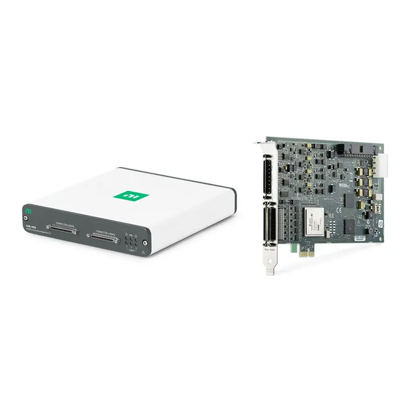
| USB-7856 | 8 AI, 8 AO, 48 DIO, 1 MS/s, USB interface | External and portable multifunction FPGA I/O |
PCIe-7856 vs PCIe-7857
The PCIe-7856 and PCIe-7857 provide similar analog and digital I/O together with a Kintex-7 160T FPGA. The principal difference is that the PCIe-7857 includes 512 MB of onboard DRAM.
Choose the PCIe-7856 when FPGA block RAM and host streaming are sufficient. Choose the PCIe-7857 when the application requires deeper onboard waveform storage or larger FPGA-side data buffers.
PCIe-7856 vs PCIe-7846
Both models provide eight analog inputs, eight analog outputs, 48 digital I/O channels and sampling rates up to 1 MS/s. The PCIe-7856 provides greater FPGA capacity for more complex processing and control.
Select the PCIe-7846 when the FPGA design is relatively small. Choose the PCIe-7856 when additional logic, DSP and block-memory resources are required.
PCIe-7856 vs PXIe-7856
The PCIe-7856 installs in a desktop or industrial computer, while the PXIe-7856 installs in a PXI Express chassis. Both use a Kintex-7 160T FPGA and provide similar multifunction I/O.
Choose the PCIe-7856 for a computer-based system. Select the PXIe-7856 when the application requires a modular PXI platform, chassis timing and integration with other PXI instruments.
Recommended Related Products
- PCIe-7857 Multifunction Reconfigurable I/O Device with DRAM
- PCIe-7858 Multifunction Reconfigurable I/O Device
- PCIe-7846 Multifunction Reconfigurable I/O Device
- PXIe-7856 Multifunction Reconfigurable I/O Module
- USB-7856 Multifunction Reconfigurable I/O Device
- PCIe-7820 Digital Reconfigurable I/O Device
- View More NI R Series Multifunction RIO Devices
- View More NI PCI and USB Data Acquisition Products
Selecting the Right R Series Device
Choose the PCIe-7856 when the application requires eight independently timed analog inputs, eight deterministic analog outputs, 48 digital channels and a Kintex-7 160T FPGA in a PCI Express computer.
Select the PCIe-7857 when onboard DRAM is required, the PXIe-7856 for PXI Express integration or the PCIe-7820 when the application requires digital FPGA I/O without analog channels.
Why Choose the PCIe-7856?
- Combines analog input, analog output and digital I/O
- Provides a dedicated ADC for every analog input
- Samples eight channels at up to 1 MS/s each
- Generates eight independent 16-bit analog outputs
- Supports 48 bidirectional digital channels
- Provides up to 80 MHz digital operation
- Supports several low-voltage logic families
- Includes a user-programmable Kintex-7 FPGA
- Enables deterministic hardware-level timing
- Supports multirate acquisition and per-channel triggering
- Provides 16 DMA channels for host transfer
- Integrates directly with PCI Express computers
Frequently Asked Questions
What is the PCIe-7856?
The PCIe-7856 is a PCI Express R Series multifunction reconfigurable I/O device with eight analog inputs, eight analog outputs, 48 digital I/O lines and a Kintex-7 FPGA.
What is the PCIe-7856 part number?
The standard NI part number for the PCIe-7856 is 786455-01.
How many analog input channels does it provide?
It provides eight 16-bit analog inputs, each with a dedicated ADC and a maximum sampling rate of 1 MS/s.
What analog input ranges are available?
The software-selectable bipolar input ranges are ±1 V, ±2 V, ±5 V and ±10 V.
How many analog outputs does the PCIe-7856 provide?
It provides eight 16-bit analog outputs with a ±10 V range and a maximum update rate of 1 MS/s.
How many digital I/O channels are available?
The device provides 48 bidirectional digital I/O lines: 16 on the multifunction connector and 32 on the high-speed digital connector.
What is the maximum digital I/O frequency?
The 32 digital lines on Connector 1 support up to 80 MHz. The 16 digital lines on Connector 0 support up to 10 MHz.
Which FPGA does the PCIe-7856 use?
It uses a Xilinx Kintex-7 160T FPGA with 101,400 lookup tables, 600 DSP48 slices and 11,700 kbits of block RAM.
Does the PCIe-7856 include onboard DRAM?
No. The PCIe-7856 has 0 MB of onboard DRAM. Consider the PCIe-7857 when 512 MB of onboard memory is required.
Can each analog input use different timing?
Yes. The dedicated ADC architecture and programmable FPGA support multirate acquisition and independent channel triggering.
Which digital logic levels are supported?
The device supports 1.2 V, 1.5 V, 1.8 V, 2.5 V and 3.3 V digital logic families.
Can the digital voltage be changed at runtime?
No. The logic voltage is selected per connector and defined when the FPGA application is compiled.
Which cables are compatible with the PCIe-7856?
The SHC68-68-RMIO cable is used for multifunction I/O, while the SHC68-C68-RDIO2 cable is recommended for high-speed digital I/O.
Which PCI Express slots are compatible?
The PCIe-7856 uses an x4 PCI Express interface and can be installed in compatible x4, x8 or x16 PCI Express slots.
Which software is required?
The device is programmed using LabVIEW and the LabVIEW FPGA Module together with compatible NI R Series Multifunction RIO drivers.
Request a Quote for the PCIe-7856
Contact us for current availability, lead time and project pricing for the PCIe-7856 Kintex-7 Multifunction Reconfigurable I/O Device. We can also help identify compatible RMIO and RDIO cables, SCB-68A terminal blocks and related PCIe, PXIe or USB R Series hardware.















