






Product Introduction
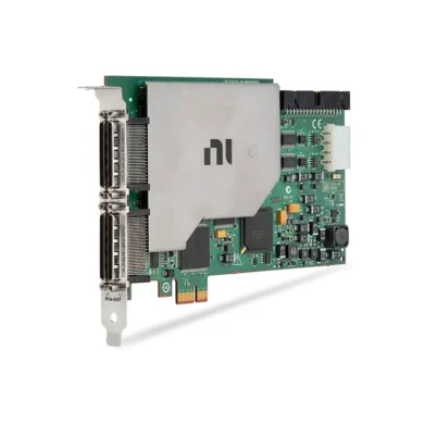
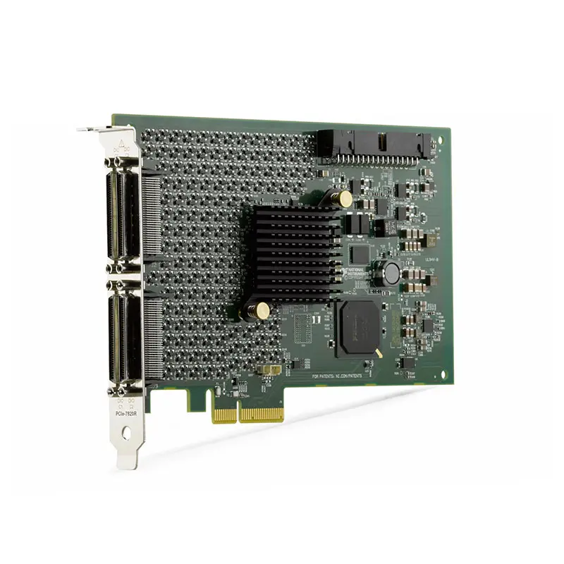
Земля NI PCIe-7820 высокопроизводительный R Series Digital Reconfigurable I/O device designed for applications requiring FPGA-based digital control, precise hardware timing, custom digital protocols, high-speed waveform generation, sensor simulation, hardware-in-the-loop testing, and automated electronic validation.
The PCIe-7820 combines a FPGA Kintex-7 160T с 128 bidirectional digital I/O channels and a PCI Express host interface. Using LabVIEW FPGA, engineers can implement custom hardware-level logic directly on the onboard FPGA.
Each digital line can be configured for functions such as digital input, digital output, counter/timer operation, PWM generation, encoder interfacing, or specialized digital communication protocols.
Product Overview
Земля National Instruments PCIe-7820 is designed for applications where conventional software-timed digital I/O does not provide sufficient timing precision, determinism, or customization.
A typical system architecture is:
Host Computer → PCI Express → PCIe-7820 → Kintex-7 FPGA → Digital I/O → DUT / Sensor / Controller
Because the user-programmable FPGA executes logic directly in hardware, the PCIe-7820 can perform deterministic digital operations independently of normal operating-system timing.
Key Features
FPGA Kintex-7 160T
The PCIe-7820 features a Xilinx Kintex-7 160T FPGA that can be programmed for custom onboard processing and digital I/O control.
FPGA functionality can be used to implement:
- Custom digital logic
- Hardware state machines
- Counter/timers
- Генерация ШИМ
- Интерфейсы энкодера
- Пользовательские протоколы связи
- Цифровое формирование сигналов
- High-speed decision making
- Hardware triggering
128 Bidirectional Digital I/O Channels
The PCIe-7820 provides 128 bidirectional digital channels.
The channels are distributed across four digital I/O connectors, providing 32 digital channels per connector.
This high channel density makes the device suitable for systems requiring large numbers of FPGA-controlled digital signals.
Up to 80 MHz Digital I/O
The digital I/O subsystem supports operation at frequencies up to 80 MHz.
This capability makes the PCIe-7820 suitable for high-speed digital control, waveform generation, protocol implementation, digital pattern generation, and other timing-sensitive applications.
Software-Selectable Logic Levels
The PCIe-7820 supports multiple digital logic voltage families:
- 1.2 V
- 1.5 V
- 1.8 V
- 2.5 V
- 3.3 V
The digital I/O voltage level is programmable by connector and defined as part of the FPGA configuration.
This flexibility allows the PCIe-7820 to interface with a wider range of modern digital electronics than fixed-voltage digital I/O devices.
Four External Clock Inputs
The PCIe-7820 provides four external clock inputs.
External clocks can be used for source-synchronous digital acquisition and other applications requiring synchronization with an external device or DUT.
Hardware-Timed FPGA Operation
The FPGA executes user-defined logic directly in hardware.
This provides deterministic operation for applications such as:
- Precise digital timing
- Custom triggering
- High-speed control loops
- Digital protocol handling
- Waveform generation
- Event response
- Signal simulation
PCI Express Interface
The PCIe-7820 installs into a compatible PCI Express slot in a desktop, workstation, rackmount, or industrial computer.
A typical architecture is:
Application Software → PCI Express → PCIe-7820 FPGA → 128 Digital I/O Channels
LabVIEW FPGA Programmability
The PCIe-7820 is designed for use with LabVIEW FPGA, allowing engineers to develop custom FPGA functionality using graphical programming.
With LabVIEW FPGA, individual digital lines can be configured for specialized functions without requiring a fixed hardware personality.
Technical Specifications
| Параметр | Спецификация |
|---|---|
| Product Type | R Series Digital Reconfigurable I/O Device |
| Модель | PCIe-7820 |
| Common Designation | PCIe-7820R |
| Manufacturer | Национальные инструменты |
| Part Number | 785361-01 |
| Шинный интерфейс | PCI Express |
| ФПГА | Кинтекс-7 160Т |
| Bidirectional Digital I/O | 128 Channels |
| Number of DIO Connectors | 4 |
| Channels per Connector | 32 |
| Maximum Digital I/O Frequency | 80 MHz |
| External Clock Inputs | 4 |
| Digital Logic Levels | 1.2 V, 1.5 V, 1.8 V, 2.5 V, 3.3 V |
| Digital Logic Compatibility | LVTTL / LVCMOS |
| FPGA Programming | LabVIEW FPGA |
| Primary Function | FPGA-Based Digital I/O and Custom Hardware Logic |
| Типичные применения | HIL, Sensor Simulation, Waveform Generation, Digital Protocols, BERT and Automated Test |
How Does the PCIe-7820 Work?
The PCIe-7820 places a user-programmable FPGA directly between the PCI Express host interface and the physical digital I/O.
A simplified architecture is:
Host Application → PCI Express → Kintex-7 FPGA → Digital I/O → DUT
Instead of requiring the host computer to control every digital transition, timing-critical logic can execute directly on the FPGA.
This reduces dependence on operating-system timing and allows deterministic hardware-level behavior.
What Is Reconfigurable I/O?
Reconfigurable I/O (RIO) allows the functionality of the hardware I/O to be defined using FPGA logic rather than being limited to a fixed instrument architecture.
For example, the same PCIe-7820 digital line can be incorporated into FPGA logic for:
- Digital input
- Digital output
- Counter
- Timer
- PWM
- Encoder input
- Запуск
- Custom protocol implementation
This flexibility is one of the primary differences between an R Series FPGA device and a conventional digital I/O card.
128-Channel Digital I/O Architecture
The PCIe-7820 provides four I/O connectors with 32 digital channels associated with each connector.
A simplified configuration is:
Connector 0 → 32 DIO Channels
Connector 1 → 32 DIO Channels
Connector 2 → 32 DIO Channels
Connector 3 → 32 DIO Channels
This provides a total of:
4 × 32 = 128 Bidirectional Digital I/O Channels
Programmable Digital Logic Levels
Different digital devices can operate at different voltage standards. The PCIe-7820 supports several software-selectable logic families to improve interface flexibility.
| Logic Level | PCIe-7820 Support |
|---|---|
| 1.2 V | Да |
| 1.5 V | Да |
| 1.8 V | Да |
| 2.5 V | Да |
| 3.3 V | Да |
The required voltage level should be selected according to the electrical requirements of the connected DUT.
High-Speed Digital Waveform Generation
NI identifies high-speed waveform generation as one of the primary applications for the PCIe-7820.
Custom FPGA logic can generate deterministic digital patterns according to application-specific timing requirements.
Typical applications can include:
- Digital stimulus generation
- Device initialization sequences
- Custom clock generation
- Digital pattern generation
- Protocol stimulus
- Automated DUT testing
Sensor Simulation
The PCIe-7820 can be used for digital sensor simulation where the sensor interface can be represented using compatible digital signals.
A typical architecture is:
Simulation Model → FPGA → PCIe-7820 Digital I/O → Controller / ECU
Custom FPGA logic can reproduce timing patterns or digital communication behavior expected from a simulated sensor.
Hardware-in-the-Loop Testing
The PCIe-7820 is well suited for hardware-in-the-loop (HIL) testing where deterministic digital signals must be exchanged with an ECU, embedded controller, or other device under test.
A typical configuration is:
HIL Application → PCIe-7820 FPGA → Digital I/O → ECU / DUT
FPGA logic can provide low-level digital stimulus, timing, protocol handling, and response processing without relying on nondeterministic software timing.
Bit Error Rate Testing
NI identifies bit error rate testing as another application for the PCIe-7820.
FPGA-based logic can generate digital patterns, acquire returned data, and implement custom comparison algorithms for digital communication validation.
A simplified architecture is:
FPGA Pattern Generator → DUT → Digital Acquisition → FPGA Comparison Logic → Test Result
Custom Digital Protocols
The user-programmable FPGA allows engineers to implement specialized digital communication protocols that may not be available on conventional interface hardware.
Potential applications include:
- Proprietary digital buses
- Custom serial communication
- Parallel digital interfaces
- Device-specific control protocols
- Specialized timing interfaces
- Legacy digital protocols
Actual implementation depends on the protocol timing, voltage levels, electrical interface, and FPGA resource requirements.
PWM Generation
Individual digital lines can be programmed through FPGA logic for pulse-width modulation (PWM) generation.
PWM applications can include:
- Motor-control signal simulation
- Actuator command simulation
- ECU testing
- Power electronics control
- Digital stimulus generation
Encoder Interface Applications
The PCIe-7820 can implement FPGA-based encoder interfaces for compatible digital encoder signals.
Custom FPGA logic can be developed for:
- Quadrature encoder inputs
- Position tracking
- Direction detection
- Pulse counting
- Speed measurement
Counter and Timer Applications
Unlike a conventional device with a fixed number of dedicated counter/timers, the PCIe-7820 allows counter and timing functions to be implemented using FPGA resources.
Possible functions include:
- Подсчет событий
- Period measurement
- Pulse-width measurement
- Frequency measurement
- Генерация импульсов
- Custom timestamping
External Clock Inputs
The PCIe-7820 provides four external clock inputs, one associated with each I/O connector.
These clock inputs can be used for source-synchronous acquisition and applications where the digital data must be sampled relative to an externally supplied clock.
The external clock source should meet the electrical and signal-quality requirements specified for the device.
Deterministic FPGA Processing
A major advantage of the PCIe-7820 is the ability to move time-critical processing from the host computer onto the FPGA.
Instead of:
Input → PC Operating System → Software Decision → Output
the system can perform:
Input → FPGA Logic → Hardware Decision → Output
This architecture is valuable for applications requiring fast, repeatable, and deterministic responses.
PCIe-7820 vs Standard Digital I/O Device
| Функция | PCIe-7820 | Standard Digital I/O Device |
|---|---|---|
| Digital Channels | 128 | Model Dependent |
| User-Programmable FPGA | Да | Usually No |
| Custom Hardware Logic | Да | Ограниченный |
| Custom Protocols | Supported Through FPGA | Usually Limited |
| PWM / Counter Functions | FPGA Configurable | Fixed Hardware Resources |
| Hardware-Level Decision Making | Да | Ограниченный |
| Primary Application | Custom Deterministic Digital I/O | General Digital I/O |
PCIe-7820 vs PXIe-7820
The PCIe-7820 and PXIe-7820 provide closely related FPGA-based digital I/O capabilities but use different host platforms.
| Функция | PCIe-7820 | PXIe-7820 |
|---|---|---|
| ФПГА | Кинтекс-7 160Т | Кинтекс-7 160Т |
| Цифровой ввод-вывод | 128 | 128 |
| Maximum DIO Frequency | 80 MHz | 80 MHz |
| Host Platform | PCI Express PC | Шасси PXI Express |
| Typical Installation | Desktop / Industrial Computer | PXIe Test System |
| Best Application | PC-Based FPGA I/O | Modular PXIe FPGA Test System |
PCIe-7820 vs PCIe-7821
The PCIe-7820 and PCIe-7821 are closely related R Series digital I/O devices based on the Kintex-7 160T FPGA.
A key selection consideration is onboard memory. The PCIe-7820 is designed without onboard DRAM, while related R Series configurations such as the PCIe-7821 include onboard DRAM.
When choosing between them, evaluate:
- FPGA requirements
- Onboard memory requirements
- Digital channel count
- Host-to-FPGA data transfer
- Waveform storage requirements
- Application architecture
PCIe-7820 vs PCIe-7822
The PCIe-7822 is another R Series digital I/O device intended for applications requiring greater FPGA resources and onboard memory.
Selection factors include:
- Required FPGA size
- FPGA logic utilization
- Onboard DRAM requirements
- Digital I/O requirements
- Custom processing complexity
- Application expansion requirements
PCIe-7820 vs Multifunction R Series Device
The PCIe-7820 is optimized for digital reconfigurable I/O. It does not provide the general-purpose analog input and analog output subsystems found on multifunction R Series devices.
| Функция | PCIe-7820 | Multifunction R Series |
|---|---|---|
| ФПГА | Да | Да |
| High-Density DIO | 128 Channels | Model Dependent |
| Analog Input | No | Да |
| Analog Output | No | Да |
| Primary Strength | Digital FPGA I/O | Mixed Analog + Digital FPGA I/O |
LabVIEW FPGA Integration
LabVIEW FPGA is used to define the hardware behavior of the PCIe-7820 FPGA.
A typical development workflow is:
- Add the PCIe-7820 FPGA target to the LabVIEW project.
- Configure the required digital I/O resources.
- Select the appropriate digital logic voltage.
- Develop the FPGA VI.
- Implement timing, state machines, counters, protocols, or control logic.
- Compile the FPGA design.
- Deploy the FPGA bitfile to the PCIe-7820.
- Communicate with the FPGA from the host application.
Digital Logic Level Configuration
The PCIe-7820 allows the digital logic level to be selected for each connector.
Supported levels include:
1.2 V / 1.5 V / 1.8 V / 2.5 V / 3.3 V
The selected logic level is defined as part of the FPGA I/O configuration and should be matched carefully to the DUT electrical requirements.
Power-Up Digital I/O Behavior
The PCIe-7820 digital I/O lines are high impedance by default during startup.
User-defined power-up behavior can be implemented through an FPGA VI when the application requires specific digital states after the FPGA configuration loads.
This is important for systems where unintended digital states could affect the connected DUT.
Cables and Connector Blocks
Compatible accessories for the PCIe-7820 include R Series high-speed digital cables and connector blocks.
Examples include:
- SHC68-C68-RDIO2 shielded R Series digital cable
- SCB-68 HSDIO shielded 68-pin connector block
Cable and terminal-block selection should be based on the required signal integrity, wiring configuration, connector type, and application bandwidth.
Legacy R Series Replacement
The PCIe-7820 can be relevant when upgrading older R Series digital I/O systems.
Before replacing an existing R Series board, verify:
- Digital I/O channel count
- Digital logic voltage
- Maximum digital frequency
- FPGA resource requirements
- Connector and cable compatibility
- Pinout
- External clock requirements
- PCI Express slot availability
- LabVIEW version
- LabVIEW FPGA compatibility
- RIO driver compatibility
- Existing FPGA VI
- FPGA compilation requirements
Older R Series FPGA code may require modification or recompilation when migrating to a different FPGA architecture.
How to Choose an R Series Digital I/O Device
Before selecting the PCIe-7820, determine:
- Required number of digital I/O channels
- Required FPGA resources
- Maximum digital operating frequency
- Required logic voltage levels
- External clock requirements
- Custom protocol requirements
- PWM and counter requirements
- Onboard DRAM requirements
- Host interface requirements
- Cable and connector requirements
- LabVIEW FPGA compatibility
- Future system expansion requirements
Industries
- Automated Test
- Automotive Testing
- Аэрокосмическая и оборонная промышленность
- Тестирование полупроводников
- Electronic Validation
- Промышленная автоматизация
- Embedded Systems
- Research and Development
- Production Test
- Hardware Validation
Applications
High-Speed Waveform Generation
The FPGA can generate custom high-speed digital patterns with deterministic hardware timing for DUT stimulus and electronic validation.
Sensor Simulation
Custom FPGA logic can simulate compatible digital sensor signals and protocols for controller and ECU testing.
Hardware-in-the-Loop Testing
The PCIe-7820 can provide deterministic digital stimulus, acquisition, protocol handling, and control for HIL test systems.
Bit Error Rate Testing
FPGA-based pattern generation and digital acquisition can support custom bit error rate testing and digital communication validation.
Custom Digital Protocols
The Kintex-7 FPGA can implement specialized or proprietary digital communication protocols that cannot be handled efficiently by conventional fixed-function digital I/O hardware.
Automated Electronic Validation
The PCIe-7820 can be integrated into automated validation systems requiring high-channel-count digital stimulus, deterministic timing, custom logic, and real-time hardware decisions.
Recommended Related Products
| PCIe-7820 | 128-channel PCI Express R Series digital I/O device with Kintex-7 160T FPGA. |
| PXIe-7820 | PXI Express version for modular FPGA-based digital I/O and automated test systems. |
| PXIe-7821 | Kintex-7 160T R Series digital I/O device with onboard DRAM for PXI Express systems. |
| PXIe-7822 | Higher-resource Kintex-7 325T R Series digital I/O device with onboard DRAM. |
| PCIe-7846 | Multifunction R Series FPGA device for applications requiring both analog and digital reconfigurable I/O. |
Why Choose PCIe-7820?
- Kintex-7 160T user-programmable FPGA
- 128 bidirectional digital I/O channels
- Four 32-channel DIO connectors
- Up to 80 MHz digital operation
- Four external clock inputs
- 1.2 V digital logic support
- 1.5 V digital logic support
- 1.8 V digital logic support
- 2.5 V digital logic support
- 3.3 V digital logic support
- LVTTL and LVCMOS compatibility
- PCI Express interface
- LabVIEW FPGA programmability
- Custom counter/timer implementation
- Генерация ШИМ
- Encoder interfacing
- Custom protocol implementation
- High-speed waveform generation
- Sensor simulation
- HIL testing
- Bit error rate testing
Frequently Asked Questions
What is the NI PCIe-7820?
The NI PCIe-7820 is a PCI Express R Series digital reconfigurable I/O device featuring a Kintex-7 160T FPGA and 128 bidirectional digital I/O channels.
What is the part number of PCIe-7820?
The NI PCIe-7820 is available under part number 785361-01.
How many digital I/O channels does PCIe-7820 have?
The PCIe-7820 provides 128 bidirectional digital I/O channels.
What FPGA does PCIe-7820 use?
The PCIe-7820 uses a FPGA Kintex-7 160T.
What is the maximum digital clock rate of PCIe-7820?
The PCIe-7820 supports a maximum digital I/O clock rate of 80 MHz.
What digital logic levels does PCIe-7820 support?
The PCIe-7820 supports software-selectable 1.2 V, 1.5 V, 1.8 V, 2.5 V, and 3.3 V digital logic levels.
How many external clock inputs does PCIe-7820 have?
The PCIe-7820 provides four external clock inputs.
Does PCIe-7820 have analog inputs?
No. The PCIe-7820 is designed as a digital R Series reconfigurable I/O device and does not provide a general-purpose analog input subsystem.
Does PCIe-7820 have analog outputs?
No. Its primary I/O subsystem consists of 128 bidirectional digital channels. Applications requiring FPGA-based analog input and output should consider an appropriate multifunction R Series device.
Can PCIe-7820 generate PWM signals?
Yes. The user-programmable FPGA can be configured to implement PWM generation using the digital I/O lines.
Can PCIe-7820 read encoder signals?
Yes. Compatible digital encoder interfaces can be implemented using custom LabVIEW FPGA logic.
Can PCIe-7820 implement custom communication protocols?
Yes. Custom digital protocols are one of the important advantages of FPGA-based R Series hardware. Protocol feasibility depends on the required electrical interface, timing, data rate, and available FPGA resources.
Can PCIe-7820 be used for HIL testing?
Yes. NI identifies hardware-in-the-loop testing as one of the primary application areas for the PCIe-7820.
Can PCIe-7820 be used for sensor simulation?
Yes. FPGA-controlled digital I/O can simulate compatible digital sensor signals and custom digital interfaces for ECU and controller testing.
Does PCIe-7820 require LabVIEW FPGA?
LabVIEW FPGA is the primary development environment used to create and compile custom FPGA functionality for the PCIe-7820. Existing applications may also deploy previously compiled FPGA bitfiles using compatible NI RIO software.
What is the difference between PCIe-7820 and PXIe-7820?
The devices provide closely related FPGA and digital I/O capabilities but use different host platforms. The PCIe-7820 installs in a compatible PCI Express computer, while the PXIe-7820 installs in a PXI Express chassis.
What is the difference between PCIe-7820 and PCIe-7821?
Both are based on the Kintex-7 160T FPGA and target high-speed reconfigurable digital I/O. One important difference is that the PCIe-7820 is a no-DRAM configuration, while related PCIe-7821 configurations include onboard DRAM.
What accessories can be used with PCIe-7820?
Compatible accessories include R Series digital cables and connector blocks such as the SHC68-C68-RDIO2 shielded cable and SCB-68 HSDIO connector block. Exact accessory compatibility should be verified for the required wiring configuration.
What should I check before purchasing PCIe-7820?
Verify the 128-channel DIO requirement, FPGA resource requirements, 80 MHz maximum digital rate, logic voltage, external clock requirements, connector and cable configuration, PCI Express compatibility, LabVIEW FPGA version, NI R Series driver support, operating system, and existing FPGA application compatibility.
Заключение
Земля NI PCIe-7820 R Series Digital Reconfigurable I/O Device combines a Kintex-7 160T FPGA, 128 bidirectional digital I/O channels, four external clock inputs, digital operation up to 80 MHz, and programmable 1.2 V to 3.3 V logic levels. Its FPGA-based architecture makes it particularly suitable for high-speed waveform generation, digital sensor simulation, hardware-in-the-loop testing, bit error rate testing, custom protocol implementation, deterministic control, and automated electronic validation.















