







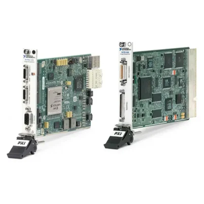

PXIe-7890 KU060 FPGA FlexRIO Multifunction I/O Module
Земля PXIe-7890 is a PXI Express FlexRIO multifunction I/O module designed for signal-level inverter hardware-in-the-loop testing. It combines eight differential analog inputs, standard analog outputs, low-latency analog outputs, 64 bidirectional digital I/O lines and two QSFP high-speed serial interfaces with a user-programmable Xilinx Kintex UltraScale KU060 FPGA.
The module provides the deterministic processing and low-latency I/O required to run traction-motor and power-electronics models directly in FPGA hardware. Engineers can use the PXIe-7890 to validate inverter controllers, motor-control ECUs and other high-speed embedded control systems under repeatable simulated operating conditions.
Key Features of the PXIe-7890
- Eight differential analog input channels
- 16-bit simultaneous analog input sampling
- 2 MS/s maximum analog input sample rate
- Programmable ±1 V, ±2 V, ±5 V, ±10 V and ±20 V input ranges
- 16 standard analog output channels
- 16 dedicated low-latency analog output channels
- 16-bit analog output resolution
- Up to 4 MS/s analog output update rate
- 64 bidirectional digital I/O channels
- Selectable 3.3 V or 5 V digital logic by 16-channel bank
- 10 MHz maximum digital output toggle rate
- Two QSFP high-speed serial interfaces
- User-programmable Xilinx Kintex UltraScale KU060 FPGA
- 331,680 FPGA lookup tables
- 2,760 DSP48 slices
- 38 Mb embedded block RAM
- 4 GB onboard DRAM
- Up to 60 DMA channels
- PXI Express timing and synchronization support
- Designed for inverter and traction-motor HIL testing
PXIe-7890 Technical Specifications
| Product Model | PXIe-7890 |
|---|---|
| Part Number | 787713-01 |
| Product Type | PXI FlexRIO multifunction I/O module |
| Primary Application | Signal-level inverter hardware-in-the-loop testing |
| ФПГА | Xilinx Kintex UltraScale KU060 |
| FPGA Lookup Tables | 331,680 |
| DSP48 Slices | 2,760 |
| Embedded Block RAM | 38 Mb |
| Onboard DRAM | 4 GB, two banks of 2 GB |
| DRAM Clock Rate | 1,064 MHz |
| Maximum Number of DMA Channels | 60 |
| Data Transfer Methods | DMA, interrupts, programmed I/O and multi-gigabit transceivers |
| FPGA Timebase Reference | PXI Express 100 MHz system clock |
| Analog Input Channels | 8 differential |
| Analog Input Resolution | 16 bits |
| Maximum Analog Input Sample Rate | 2 MS/s |
| Analog Input Sampling | Синхронный |
| Analog Input Ranges | ±1 V, ±2 V, ±5 V, ±10 V and ±20 V |
| Analog Input Filtering | Programmable low-latency filtering |
| Published Analog Input Absolute Accuracy | 0.71 mV for the applicable range and conditions |
| Standard Analog Output Channels | 16 |
| Low-Latency Analog Output Channels | 16 |
| Total Analog Output Channels | 32 |
| Analog Output Resolution | 16 bits |
| Maximum Analog Output Update Rate | 4 MS/s |
| Standard Analog Output Range | ±10 V |
| Low-Latency AO Channels 0 through 7 | ±10 V and ±0.5 V ranges |
| Low-Latency AO Channels 8 through 15 | ±10 V range |
| Standard AO Uncalibrated Update Latency | 440 ns |
| Standard AO Calibrated Update Latency | 460 ns |
| Standard AO Analog Latency | 75 ns |
| Low-Latency AO Uncalibrated Update Latency | 148 ns |
| Low-Latency AO Calibrated Update Latency | 168 ns |
| Low-Latency AO Analog Latency | 50 ns |
| Bidirectional Digital I/O Channels | 64 |
| Digital I/O Signal Type | Single-ended |
| Digital Logic Levels | 3.3 V or 5 V, selectable by 16-channel bank |
| Digital Direction Control | Per channel |
| Maximum Digital Output Current | 4 mA sink or source per channel |
| Maximum Digital Output Toggle Rate | 10 MHz |
| High-Speed Serial Connectors | 2 × QSFP |
| Primary I/O Connectors | Multiple 68-pin VHDCI receptacles |
| Шинный интерфейс | PXI Express |
| Reconfigurable | Да |
| Operating Temperature | 0°C to 55°C |
| Calibration Interval | 2 years |
PXIe-7890 Part Number and Calibration Accessory
| Item | Part Number | Описание |
|---|---|---|
| PXIe-7890 | 787713-01 | KU060 FPGA multifunction FlexRIO module with analog I/O, digital I/O and QSFP interfaces |
| CAL-7890/7891 Calibration Fixture | 788790-01 | Calibration fixture for PXIe-7890 and PXIe-7891 signal-level HIL modules |
The PXIe-7890 uses several front-panel connectors for its different I/O resources. Verify the required VHDCI breakout assemblies, QSFP cables, logic voltage, connector pinout and test-fixture wiring before ordering.
Signal-Level Inverter HIL Architecture
The PXIe-7890 is designed to connect a real inverter controller or motor-control ECU to a simulated power stage and traction motor. The actual high-voltage inverter and motor are replaced by mathematical models running deterministically on the FPGA.
Analog inputs acquire controller feedback and command signals, while low-latency analog outputs return simulated current, voltage, resolver or other sensor information. Digital I/O and high-speed serial interfaces support additional feedback, communication and synchronization requirements.
Xilinx Kintex UltraScale KU060 FPGA
The user-programmable KU060 FPGA provides the parallel processing resources required for deterministic power-electronics and motor-model execution. Calculations can operate directly between the input and output interfaces without relying on nondeterministic host-software timing.
The FPGA includes 331,680 lookup tables, 2,760 DSP48 slices and 38 Mb of embedded block RAM. These resources support custom control logic, signal processing, plant models, communication protocols and high-speed closed-loop calculations.
Some FPGA resources are reserved by the module interface and PCI Express infrastructure, so the resources available to a user application are slightly lower than the FPGA’s total physical capacity.
Eight Simultaneous Analog Inputs
The PXIe-7890 provides eight differential analog input channels with 16-bit resolution and simultaneous sampling. Each channel can acquire at up to 2 MS/s.
Simultaneous conversion helps preserve the timing relationship between phase-current, DC-bus, command and feedback signals. This is important for multichannel control models that use several measurements during the same FPGA calculation step.
Programmable Analog Input Ranges
The analog inputs support selectable ranges of ±1 V, ±2 V, ±5 V, ±10 V and ±20 V. The range can be matched to the expected signal amplitude to balance headroom and measurement resolution.
Use the smallest range that safely contains the complete signal, including normal transients and possible fault conditions. Do not rely on the selected measurement range as overvoltage protection.
Programmable Low-Latency Input Filtering
Programmable input filtering can reduce unwanted noise and aliasing while supporting the low latency required by real-time HIL models. Filter configuration should reflect the signal bandwidth and FPGA loop rate.
Excessive filtering can add phase delay or suppress legitimate transient behavior. Validate the complete measurement path against the control system’s frequency-response requirements.
Standard Analog Outputs
The standard analog outputs provide 16-bit voltage generation with a ±10 V range. They are suitable for simulated sensor outputs, references, diagnostic signals and other voltage commands that do not require the module’s shortest output latency.
Standard output latency includes the FPGA update path and analog circuitry. Total hardware latency is determined by adding the applicable update latency and analog latency.
Low-Latency Analog Outputs
The 16 low-latency analog outputs are optimized for fast signal-level HIL feedback. Their reduced update latency helps shorten the closed-loop delay between acquiring an ECU signal, executing the FPGA model and returning the simulated response.
Channels 0 through 7 support both ±10 V and ±0.5 V ranges. Channels 8 through 15 support the ±10 V range. The smaller range can improve useful resolution for low-amplitude feedback signals.
Understanding Analog Output Latency
Total analog output latency consists of update latency plus analog latency. Calibrated operation applies stored scaling coefficients and therefore has slightly longer update latency than uncalibrated operation.
| Тип вывода | Uncalibrated Total Latency | Calibrated Total Latency |
|---|---|---|
| Standard analog output | Approximately 515 ns | Approximately 535 ns |
| Low-latency analog output | Approximately 198 ns | Approximately 218 ns |
These figures describe the applicable hardware output path. The complete closed-loop latency also includes analog input conversion, FPGA model execution, synchronization and any external signal-conditioning delay.
64 Bidirectional Digital I/O Channels
The PXIe-7890 provides 64 single-ended digital I/O lines distributed across two 68-pin VHDCI connectors. Each connector carries half of the total digital channels.
Direction is configurable per channel, allowing the FPGA application to combine inputs and outputs according to the test-system requirements. Digital signals can represent PWM states, enable commands, fault lines, encoder signals and general ECU control I/O.
Selectable 3.3 V and 5 V Logic
The digital logic level can be selected as 3.3 V or 5 V in banks of 16 channels. All lines within a voltage bank use the same selected logic family.
Confirm the required voltage before connecting the device under test. Applying an incompatible logic level may result in unreliable operation or damage to the PXIe-7890 or ECU.
10 MHz Digital Output Operation
Digital outputs support a maximum toggle rate of 10 MHz and can sink or source up to 4 mA per channel. This capability supports many control, status and moderate-speed pulse applications.
The digital I/O is not intended to drive high-current loads directly. Use suitable buffers, level translators or external drivers when the connected circuit requires more current or a different electrical standard.
Two QSFP High-Speed Serial Interfaces
Two QSFP connectors provide high-speed serial communication through the FPGA’s multi-gigabit transceivers. These ports can exchange data with compatible FPGA modules, simulation hardware or custom interfaces.
The exact line rate, protocol and channel configuration depend on the FPGA design and connected equipment. Cable type, transceiver compatibility and link configuration must be confirmed for the intended application.
Aurora Protocol Support
NI provides an Aurora-based sample project and CLIP for the PXIe-7890. This reference design can be used as a starting point for low-overhead, high-speed serial communication through the QSFP interfaces.
The example can be generated using the FlexRIO Integrated I/O Getting Started example in LabVIEW. Application-specific FPGA development is still required to integrate the link with the final motor model or HIL architecture.
4 GB Onboard DRAM
The module includes 4 GB of onboard DRAM divided into two 2 GB banks. The memory can buffer waveform data, model parameters, lookup tables and other information used by the FPGA application.
Efficient memory access is important when the FPGA model requires high throughput. The achievable application bandwidth depends on access patterns, FPGA design and competition between memory clients.
DMA Data Transfer
Up to 60 DMA channels can transfer data between the FPGA and host memory. DMA can be used for waveform streaming, test data capture, configuration updates and diagnostic information.
The host controller, PXI Express chassis topology and other modules sharing the bus affect sustainable data-transfer performance. Critical HIL feedback loops should remain in FPGA hardware rather than depend on host communication.
Traction-Motor Model Execution
The KU060 FPGA can execute mathematical models representing traction motors, including electrical and mechanical behavior. Multiple model components can operate in parallel to achieve short deterministic time steps.
The exact number and complexity of motor models depend on the selected model, numerical method, FPGA clock rate, resource usage and I/O requirements.
Inverter Controller Validation
The PXIe-7890 can validate an inverter controller without connecting it to a high-power inverter and motor. The controller receives simulated feedback while its commands are captured and evaluated by the FPGA model.
This arrangement helps test normal operation, startup, shutdown, torque commands, speed transitions and error handling in a controlled laboratory environment.
Electric Vehicle Powertrain Testing
Electric vehicle test systems can use the module to simulate traction-motor and inverter behavior at signal level. The real ECU executes its production control software while the FPGA recreates the response of the electrical powertrain.
Signal-level testing reduces the risk and energy associated with testing every software condition on a physical high-voltage dynamometer.
Fault and Corner-Case Simulation
FPGA logic can introduce simulated overcurrent, overspeed, sensor offset, missing feedback and other abnormal operating conditions. These repeatable scenarios help verify diagnostic and protective behavior.
Electrical faults that require changing actual ECU wiring or applying abnormal voltages may require separate fault insertion and signal-conditioning hardware.
ECU Regression Testing
Automated regression systems can replay the same operating profiles after software or calibration changes. Consistent simulated conditions make differences between ECU versions easier to identify.
Test sequences can record analog measurements, digital states, model variables and diagnostic results for comparison and reporting.
PXI Timing and Synchronization
The FPGA can use the PXI Express 100 MHz reference clock. PXI timing and triggering resources allow the module to coordinate with data acquisition, communication, fault insertion and measurement instruments.
Shared timing is valuable when inverter commands, simulated feedback, network messages and external measurements must be correlated on a common timebase.
LabVIEW FPGA Integration
LabVIEW FPGA allows engineers to create custom deterministic processing and I/O logic for the KU060 FPGA. The application can implement plant models, control interfaces, triggers, fault logic and custom serial communication.
FPGA development requires compatible LabVIEW FPGA and FlexRIO software. Confirm software-version, operating-system, controller and compilation-service compatibility before configuring the system.
LabVIEW Real-Time Integration
A compatible PXI real-time controller can manage test sequencing, parameter updates, network communication, data logging and interaction with the FPGA model.
Time-critical calculations remain on the FPGA, while the real-time controller handles tasks that require deterministic sequencing but do not need submicrosecond execution.
Typical PXIe-7890 Applications
- Signal-level inverter HIL testing
- Traction-motor controller validation
- Electric vehicle powertrain development
- Motor-control ECU regression testing
- Power-electronics controller verification
- FPGA-based plant simulation
- Resolver and sensor signal simulation
- PWM command acquisition
- Fault and corner-case simulation
- Closed-loop embedded controller testing
- Rapid control prototyping
- Custom high-speed serial communication
- Multichannel deterministic signal generation
- Automotive and aerospace controller testing
PXIe-7890 Troubleshooting
The PXIe-7890 is not detected in NI MAX
Confirm that the module is fully installed in a compatible PXI Express slot. Check chassis power, controller communication and FlexRIO driver installation, then restart the system and rescan the hardware.
The FPGA bitfile cannot be loaded
Verify that the bitfile was compiled for the PXIe-7890 and KU060 target. Confirm compatibility between the bitfile, FlexRIO driver, LabVIEW FPGA version and host application.
An analog input signal is clipped
Check the selected input range and actual signal amplitude. Select a larger range when the signal, including transients and offset, exceeds the configured limits.
Analog input data contains excessive noise
Review grounding, shielding, differential wiring and filter configuration. Keep low-level analog wiring separated from digital and switching-power signals.
A low-latency analog output does not use the ±0.5 V range
The ±0.5 V range is available only on low-latency channels 0 through 7. Low-latency channels 8 through 15 support the ±10 V range.
Analog output latency is higher than expected
Confirm whether calibrated or uncalibrated mode is used. Include both update latency and analog latency, as well as FPGA computation and synchronization delays.
Digital I/O uses the wrong logic voltage
Check the voltage selection for the corresponding 16-channel bank. All channels in the bank must use the same 3.3 V or 5 V logic setting.
A digital output cannot drive the connected load
The maximum output current is 4 mA per channel. Use an external buffer or driver for loads requiring more current.
The QSFP serial link does not establish communication
Verify cable and transceiver compatibility, FPGA protocol configuration, line rate, reference clock and lane assignment. Confirm that both ends use compatible Aurora or custom serial-link settings.
Host streaming throughput is lower than expected
Review DMA configuration, chassis PCI Express topology, controller performance and traffic from other modules. Keep deterministic closed-loop calculations on the FPGA.
The HIL model cannot meet its required loop rate
Review FPGA timing reports, resource utilization, memory access and arithmetic architecture. Pipeline the calculations, parallelize independent operations or simplify the numerical model where appropriate.
PXIe-7890 Comparison with Related FPGA Modules
| Модель | Primary Configuration | Best Suited For |
|---|---|---|
| PXIe-7890 | KU060 FPGA, analog I/O, low-latency AO, 64 DIO and 2 QSFP | Signal-level inverter and traction-motor HIL |
| PXIe-7891 | Signal-level HIL FPGA multifunction architecture | Related HIL systems requiring the PXIe-7891 I/O configuration |
| PXIe-7981 | Related FPGA-based HIL and high-speed serial platform | Applications requiring its specific FPGA and interface resources |
| PXIe-7915 | FlexRIO FPGA coprocessor | Custom FPGA processing with separately selected I/O modules |
| PXIe-7868 | Multifunction reconfigurable I/O | General-purpose FPGA control and lower-complexity HIL systems |
PXIe-7890 vs General-Purpose FlexRIO Modules
The PXIe-7890 integrates analog inputs, standard and low-latency analog outputs, digital I/O and high-speed serial ports for signal-level inverter HIL. General FlexRIO FPGA modules may require separately selected adapter modules or additional signal-conditioning hardware.
Choose the PXIe-7890 when its integrated I/O combination matches a motor-control or power-electronics test application. Select a general-purpose FlexRIO platform when a different analog, digital or RF interface must be combined with FPGA processing.
PXIe-7890 vs PXIe-7891
The PXIe-7890 and PXIe-7891 belong to the same signal-level HIL FPGA product family. Their exact I/O resources and intended system roles should be compared against the required motor models, feedback signals, digital channels and serial interfaces.
Select the model only after confirming the official pinout, FPGA design target, breakout hardware and software examples required by the HIL application.
Recommended Related Products
- PXIe-7891 Signal-Level HIL FlexRIO Module
- PXIe-7981 FPGA HIL Module
- PXIe-7915 FlexRIO FPGA Coprocessor Module
- PXIe-7868 Multifunction Reconfigurable I/O Module
- View More NI PXI and PXI Express Modules
Selecting the Right HIL FPGA Module
Choose the PXIe-7890 when the application requires eight simultaneous analog inputs, standard and low-latency analog outputs, 64 bidirectional digital channels, QSFP serial connectivity and a KU060 FPGA.
Before ordering, confirm the number and type of analog outputs, voltage ranges, DIO logic voltage, FPGA resource requirements, QSFP protocol, connector pinout and compatible software versions.
Why Choose the PXIe-7890?
- Integrates analog, digital and serial I/O in one FPGA module
- Provides low-latency analog feedback for inverter HIL
- Includes eight simultaneous 16-bit analog inputs
- Provides 32 total analog output channels
- Offers 64 configurable digital I/O lines
- Supports 3.3 V and 5 V digital logic
- Includes two QSFP serial interfaces
- Uses a powerful Kintex UltraScale KU060 FPGA
- Provides 4 GB of onboard DRAM
- Supports PXI timing and LabVIEW FPGA customization
Frequently Asked Questions
What is the PXIe-7890?
The PXIe-7890 is an FPGA-based PXI FlexRIO multifunction I/O module designed primarily for signal-level inverter and traction-motor hardware-in-the-loop testing.
What is the PXIe-7890 part number?
The standard NI part number for the PXIe-7890 is 787713-01.
Which FPGA does the module use?
The PXIe-7890 uses a user-programmable Xilinx Kintex UltraScale KU060 FPGA.
How many analog inputs does it provide?
The module provides eight simultaneously sampled differential analog inputs with 16-bit resolution and rates up to 2 MS/s.
Which analog input ranges are supported?
The selectable input ranges are ±1 V, ±2 V, ±5 V, ±10 V and ±20 V.
How many analog outputs does the PXIe-7890 provide?
The detailed hardware configuration provides 16 standard analog outputs and 16 low-latency analog outputs, for 32 total voltage-output channels.
What is the maximum analog output update rate?
The maximum published analog update rate is 4 MS/s.
Which low-latency outputs support the ±0.5 V range?
Low-latency channels 0 through 7 support both ±0.5 V and ±10 V ranges. Channels 8 through 15 support ±10 V.
How many digital I/O channels are available?
The module provides 64 bidirectional, single-ended digital I/O channels.
Does the DIO support 3.3 V and 5 V logic?
Yes. Logic voltage is selectable as 3.3 V or 5 V for each group of 16 digital channels.
What is the maximum digital output current?
Each digital output can sink or source up to 4 mA.
What are the QSFP ports used for?
The two QSFP ports expose FPGA multi-gigabit serial resources for Aurora or other application-specific high-speed communication.
How much onboard DRAM does the module provide?
The PXIe-7890 includes 4 GB of onboard DRAM organized as two 2 GB banks.
Does the PXIe-7890 support Aurora?
Yes. NI provides an Aurora-based sample project and CLIP that can be generated through the FlexRIO Integrated I/O Getting Started example.
Which software is required?
The module uses NI FlexRIO software and can be programmed with LabVIEW FPGA. A compatible LabVIEW Real-Time environment may also be used for complete HIL systems.
What is the recommended calibration interval?
The published calibration interval is two years.
Request a Quote for the PXIe-7890
Contact us for current availability, lead time and project pricing for the PXIe-7890 KU060 FPGA FlexRIO Multifunction I/O Module. We can also help confirm the calibration fixture, compatible PXI Express chassis, VHDCI and QSFP connectivity, software requirements and related FPGA modules for your inverter HIL system.















