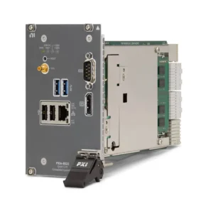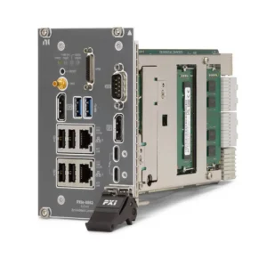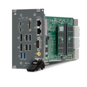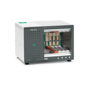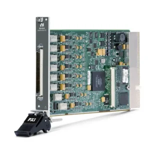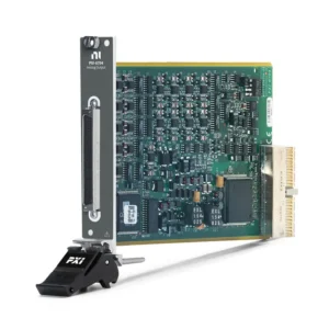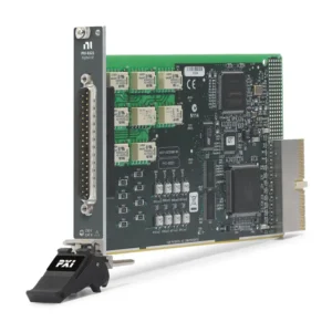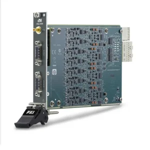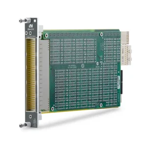


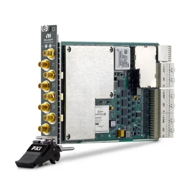
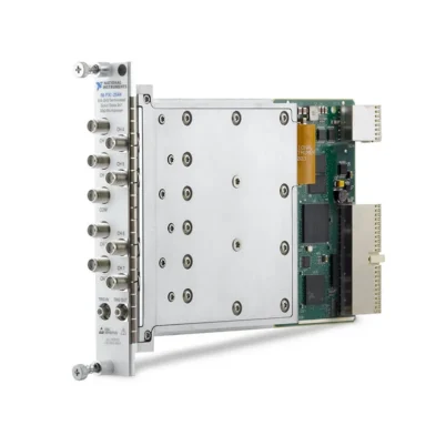
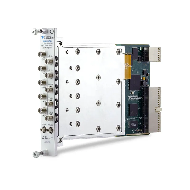
PXI-2543 6.6 GHz Dual 4×1 Solid-State RF Multiplexer
Земля PXI-2543 is a dual-bank, terminated 4×1 PXI RF multiplexer switch module designed for automated RF and microwave signal routing. It contains two independent 4×1 multiplexers, allowing two common ports to select between four RF channels in each bank.
With a frequency range from 10 MHz to 6.6 GHz, 50 Ω nominal impedance and fast solid-state FET switching, the PXI-2543 is suitable for wireless device testing, RF semiconductor characterization, signal-generator routing, analyzer input selection and high-throughput production testing.
Every channel and common port includes internal 50 Ω termination. This helps maintain a defined impedance for disconnected ports, reduce reflections and protect sensitive RF sources and devices during route changes.
Key Features of the PXI-2543
- Two independent 4×1 RF multiplexer banks
- Eight RF input or output channels
- Two common RF ports
- 10 MHz to 6.6 GHz operating frequency range
- 50 Ω nominal characteristic impedance
- Internally terminated channels and common ports
- High-performance solid-state FET switching
- No mechanical relay-contact wear
- Approximately 76 µs switching time
- +30 dBm maximum continuous RF power with chassis power on
- +20 dBm maximum continuous RF power with chassis power off
- ±8 V maximum safe DC voltage
- AC-coupled RF signal paths
- High RF isolation through 6.6 GHz
- Less than 10 ps typical channel-to-channel skew
- Ten front-panel SMA RF connectors
- Separate SMB trigger input and output connectors
- NI-SWITCH and NI Switch Executive compatibility
PXI-2543 Technical Specifications
| Product Model | PXI-2543 |
|---|---|
| Part Number | 778572-43 |
| Product Type | PXI RF multiplexer switch module |
| Topology | Dual 4×1 terminated multiplexer |
| Number of Banks | 2 independent banks |
| Channels per Bank | 4 |
| Total RF Channels | 8 channels plus 2 common ports |
| Диапазон частот | 10 MHz to 6.6 GHz |
| Characteristic Impedance | 50 Ω nominal |
| Coupling | AC coupled |
| Switch Type | Solid-state FET |
| Port Termination | Internal 50 Ω termination on every channel and common port |
| Maximum Safe DC Voltage | ±8 V |
| Maximum Continuous RF Power | +30 dBm with chassis power on |
| Maximum RF Power with Chassis Off | +20 dBm |
| Insertion Loss to 2.4 GHz | Less than 4.1 dB |
| Insertion Loss to 6 GHz | Less than 5.8 dB |
| Insertion Loss to 6.6 GHz | Less than 7.0 dB |
| VSWR to 2.4 GHz | Less than 1.7; less than 1.5 typical |
| VSWR to 6 GHz | Less than 1.8; less than 1.5 typical |
| VSWR to 6.6 GHz | Less than 2.4; less than 1.6 typical |
| Channel-to-Common Isolation to 2.4 GHz | Greater than 70 dB; greater than 84 dB typical |
| Channel-to-Common Isolation to 6 GHz | Greater than 61 dB; greater than 74 dB typical |
| Channel-to-Common Isolation to 6.6 GHz | Greater than 59 dB; greater than 72 dB typical |
| Channel-to-Channel Isolation to 6.6 GHz | Greater than 53 dB; greater than 71 dB typical |
| Bank-to-Bank Crosstalk | Less than -90 dB typical |
| Channel-to-Channel Skew | Less than 10 ps typical |
| Propagation Delay | 1,720 ps typical |
| Input 1 dB Compression | Greater than +27.6 dBm minimum; greater than +32 dBm typical |
| Typical Input IP2 | Greater than +89 dBm |
| Typical Input IP3 | Greater than +54 dBm |
| Switching Time | Approximately 76 µs |
| Input Trigger | Front-panel TRIG IN and supported PXI trigger resources |
| Output Trigger | Front-panel TRIG OUT and supported PXI trigger resources |
| Minimum Input Trigger Pulse Width | 150 ns |
| RF Connectors | 10 female SMA jacks |
| Trigger Connectors | 2 female SMB jacks |
| Поддержка программного обеспечения | NI-SWITCH and NI Switch Executive |
| Шинный интерфейс | PXI |
| Module Format | 3U, single-slot PXI module |
| Dimensions | 21.6 × 2.0 × 13.0 cm |
| Weight | Approximately 774 g |
| Operating Temperature | 0°C to 55°C |
| Storage Temperature | -20°C to 70°C |
| Product Status | Discontinued by NI |
PXI-2543 Part Number and Accessories
| Item | Part Number | Описание |
|---|---|---|
| PXI-2543 | 778572-43 | 6.6 GHz, 50 Ω, terminated dual 4×1 PXI RF multiplexer |
| SMA 100 Cable | 763443-01 | 0.15 m flexible SMA male-to-SMA male RF cable |
| SMA 100 Cable | 763444-01 | 0.45 m flexible SMA male-to-SMA male RF cable |
| SMA 50 Ω Termination Plug | 778353-01 | External 50 Ω termination for compatible SMA RF connections |
| RF Torque Screwdriver and SMA Driver Bit | 780895-01 | Torque tool for installing compatible SMA cables |
| RF SMA Driver Bit | 780894-01 | SMA driver bit for compatible torque tools |
The PXI-2543 uses front-panel SMA connectors for RF signals and SMB connectors for trigger input and output. Use 50 Ω cables rated for the required frequency and apply the manufacturer-recommended connector torque.
Dual 4×1 Multiplexer Architecture
The PXI-2543 contains two independent RF multiplexer banks identified as Bank A and Bank B. Each bank provides four selectable channels and one common connection.
Bank A includes CH 0A through CH 3A and COM A. Bank B includes CH 0B through CH 3B and COM B. Software can independently select a channel in each bank, allowing two RF routes to operate simultaneously.
The dual-bank architecture is useful when a test system must route both a stimulus and response signal or control two separate RF signal paths within the same PXI module.
Terminated RF Multiplexer Design
Every channel and common connection includes internal 50 Ω termination. When a port is not selected, the termination maintains a defined impedance instead of leaving the port open.
This design can reduce reflections, stabilize connected RF sources and simplify test systems in which unused ports must remain terminated. It is particularly useful for signal generators, amplifiers and devices that require a consistent 50 Ω load.
The internal terminations dissipate RF energy, so all applied signals must remain within the published power ratings, including signals connected to currently unselected channels.
10 MHz to 6.6 GHz Frequency Range
The PXI-2543 routes RF signals from 10 MHz to 6.6 GHz. This frequency range covers many cellular, WLAN, Bluetooth, GNSS, ISM-band, satellite intermediate-frequency and general RF test applications.
The module is AC coupled and is not intended for switching DC or very-low-frequency measurement signals. The ±8 V DC rating is a maximum safe limit rather than a supported DC-routing specification.
Solid-State FET Switching
The PXI-2543 uses solid-state FET switches rather than electromechanical relays. This architecture eliminates mechanical contact wear and supports very high switching-cycle counts.
Solid-state switching is valuable in production systems that reconfigure RF routes frequently. It also provides faster and more repeatable switching than many electromechanical microwave relays.
Unlike an ideal mechanical contact, a solid-state RF path introduces frequency-dependent insertion loss, compression and nonlinear distortion. These characteristics should be considered when testing low-level or high-dynamic-range RF signals.
Fast Switching Time
The solid-state architecture provides an approximate switching time of 76 µs. This allows the module to move rapidly between RF channels during automated measurements.
Overall test throughput also depends on signal-source settling, device-under-test response, analyzer acquisition time, trigger configuration and measurement processing.
RF Power Handling
All RF ports are marked for a maximum level of +30 dBm while the PXI chassis is powered. +30 dBm corresponds to 1 W in a 50 Ω system.
When chassis power is removed, maximum continuous RF power is reduced to +20 dBm. Disconnect or reduce external RF signals before powering down the chassis when they could exceed the unpowered limit.
Peak, pulsed and multitone signals must be evaluated using their actual peak voltage and power. Do not rely only on average power when the waveform has a high peak-to-average ratio.
Insertion Loss
Insertion loss increases with frequency. The specified maximum is less than 4.1 dB through 2.4 GHz, less than 5.8 dB through 6 GHz and less than 7.0 dB through 6.6 GHz.
The complete path loss also includes SMA cables, adapters, fixtures and connector wear. For amplitude-sensitive testing, characterize each route and apply frequency-dependent path-loss correction.
Insertion loss also changes with temperature. Systems requiring tight amplitude accuracy should allow the PXI chassis to warm up and should calibrate the complete RF path under representative operating conditions.
VSWR and Impedance Matching
The PXI-2543 has a nominal 50 Ω impedance. Typical VSWR remains below 1.5 through 6 GHz and below 1.6 through 6.6 GHz.
Use high-quality 50 Ω cables and properly torqued SMA connectors to preserve return-loss performance. Damaged connectors, loose interfaces and unnecessary adapters can create reflections and measurement error.
RF Isolation
Channel-to-common isolation is typically greater than 84 dB through 2.4 GHz, greater than 74 dB through 6 GHz and greater than 72 dB through 6.6 GHz.
Channel-to-channel isolation is typically greater than 90 dB through 2.4 GHz, greater than 74 dB through 6 GHz and greater than 71 dB through 6.6 GHz.
High isolation helps prevent signals on inactive channels from leaking into the selected RF route. Actual system isolation can be limited by external cable coupling, fixtures, grounding and connected instruments.
Bank-to-Bank Crosstalk
Typical crosstalk between Bank A and Bank B is below -90 dB. This supports applications where the two multiplexer banks carry different RF signals simultaneously.
For the best system-level isolation, physically separate high-power and low-level external cables and avoid routing them in long parallel bundles.
Low Propagation Delay and Skew
Typical propagation delay is approximately 1,720 ps, and typical channel-to-channel skew is less than 10 ps. These characteristics help maintain timing repeatability when selecting between comparable RF paths.
External cable length can introduce substantially more delay and skew than the module. Use phase-matched cables when phase or timing alignment is important.
RF Linearity
The PXI-2543 provides a typical input 1 dB compression point above +32 dBm, with a specified minimum above +27.6 dBm. Typical input IP2 is greater than +89 dBm, and typical input IP3 is greater than +54 dBm.
These specifications help engineers estimate distortion when routing high-level or multitone RF signals. The applied signal must still remain within the module’s maximum safe power and voltage limits.
SMA RF Connections
The front panel provides ten female SMA connectors: four channel ports and one common port for each of the two multiplexer banks.
SMA connectors should be tightened with a suitable torque tool rather than hand-tightened or overtightened. Consistent connector torque improves measurement repeatability and reduces connector damage.
Front-Panel Triggering
Separate TRIG IN and TRIG OUT SMB connectors support external synchronization. The module can also use supported PXI backplane triggering resources.
Hardware triggering allows channel selection to be coordinated with RF generators, digitizers, analyzers and other instruments without relying entirely on software timing.
NI-SWITCH Software Support
The PXI-2543 is controlled through the NI-SWITCH instrument driver. NI-SWITCH provides functions for initialization, channel connection, disconnection, scanning, triggering and switch-status management.
The driver supports LabVIEW, LabWindows/CVI and compatible text-based programming environments. Verify driver and operating-system compatibility when installing the module in an older PXI controller.
NI Switch Executive Integration
NI Switch Executive allows engineers to define descriptive route names instead of controlling individual physical relay names directly. This makes automated test code easier to understand and maintain.
Named routes are particularly useful when the PXI-2543 operates with additional RF switches, signal generators, analyzers and device-interface fixtures.
Typical PXI-2543 Applications
- Wireless device production testing
- RF semiconductor characterization
- Cellular transmitter and receiver testing
- WLAN and Bluetooth device testing
- Signal-generator output selection
- Spectrum-analyzer input routing
- RF digitizer channel selection
- Power-amplifier testing
- RF front-end module validation
- Antenna and receiver testing
- Multiband radio validation
- Automated RF calibration systems
- Parallel RF production testing
- Laboratory microwave signal routing
Тестирование беспроводных устройств
The PXI-2543 can route RF stimulus and response signals for cellular, WLAN, Bluetooth and other wireless-device tests. One bank can select a generator or transmitter path while the other bank selects an analyzer or receiver path.
The 6.6 GHz upper frequency limit supports many sub-6 GHz communications bands. Apply path-loss correction when accurate transmit power or receiver sensitivity measurements are required.
RF Semiconductor Testing
The dual multiplexer banks can connect RF semiconductor devices to generators, analyzers, power meters and other instruments during characterization or production testing.
Solid-state switching supports frequent channel changes without mechanical contact wear, which is useful in high-volume semiconductor test systems.
Signal Generator and Analyzer Routing
A common port can connect one RF instrument to any of four device or fixture connections. The second bank can provide an independent return or measurement path.
Because unused ports are terminated, connected sources see a defined impedance even when they are not selected. Confirm that the internal termination can safely dissipate the applied signal power.
PXI-2543 Troubleshooting
The PXI-2543 Is Not Detected in NI MAX
Confirm that the module is fully seated in a compatible PXI or hybrid slot. Check chassis power, controller communication and NI-SWITCH installation, then restart the system and rescan for hardware.
No RF Signal Reaches the Common Port
Verify that the correct bank and channel are selected. Check the SMA cable, source output, common-port connection and NI-SWITCH route name.
The Signal Level Is Lower Than Expected
Account for the PXI-2543 insertion loss and all external cable and fixture loss. Because insertion loss increases with frequency, use frequency-dependent correction rather than one fixed offset.
The Measurement Has Excessive Reflections
Confirm that all external equipment and cables use 50 Ω impedance. Inspect and correctly torque the SMA connectors, then remove unnecessary adapters or damaged cables.
An Unselected Signal Appears at the Common Port
Check channel-to-channel coupling in the external fixture and cables. Strong RF signals can leak through external components even when the module meets its isolation specifications.
The RF Signal Is Present When Chassis Power Is Off
Remove or reduce the signal before powering down the chassis. Maximum continuous RF power falls from +30 dBm with power on to +20 dBm with power off.
The Trigger Does Not Change Channels
Verify the trigger source, trigger destination, SMB cable, polarity and pulse width. Confirm that the scan list or triggered switching operation is initiated before the trigger arrives.
Measurements Differ Between Channels
Characterize each complete route separately. Channel-to-channel variation may include switch loss, cable loss, connector repeatability and fixture response.
High-Power Signals Produce Distortion
Check the signal’s peak power, compression requirements and multitone characteristics. Reduce the input level and confirm that the signal remains within both the maximum safe rating and required linearity range.
PXI-2543 Comparison with Similar RF Switch Modules
| Модель | Primary Configuration | Best Suited For |
|---|---|---|
| PXI-2542 | 6.6 GHz dual 4×1 solid-state RF multiplexer | Applications requiring an unterminated switching topology |
| PXI-2543 | 6.6 GHz terminated dual 4×1 solid-state RF multiplexer | Fast RF routing with every channel and common port terminated |
| PXIe-2543 | 6.6 GHz terminated dual 4×1 PXI Express RF multiplexer | Current PXI Express systems requiring the same terminated architecture |
| PXI-2544 | 6.6 GHz solid-state RF multiplexer architecture | Applications requiring a different channel and common-port arrangement |
| PXI-2547 | High-frequency RF multiplexer with electromechanical switching | Applications prioritizing low insertion loss and relay isolation |
| PXI-2598 | Dual-transfer RF switch architecture | Swapping two RF signal paths rather than multiplexing four channels |
PXI-2543 vs PXI-2542
The PXI-2543 provides internal 50 Ω termination on each channel and common port. The PXI-2542 uses a related solid-state RF switching architecture but is intended for applications that require an unterminated configuration.
Choose the PXI-2543 when disconnected ports must remain terminated to reduce reflections or provide a defined load. Consider the PXI-2542 when the external system provides its own termination or requires the unselected paths to remain unterminated.
PXI-2543 vs PXIe-2543
The PXI-2543 and PXIe-2543 provide the same basic terminated dual 4×1 topology, 6.6 GHz bandwidth, 50 Ω impedance and solid-state switching architecture.
The PXI-2543 uses the traditional PXI interface and part number 778572-43. The PXIe-2543 uses the PXI Express interface and part number 780587-43. Verify chassis slot compatibility before selecting a replacement.
Solid-State vs Electromechanical RF Switching
The solid-state PXI-2543 offers fast operation and avoids mechanical contact wear. This makes it suitable for applications requiring a very high number of switching cycles.
Electromechanical RF switches may provide lower insertion loss, higher off-state isolation or different power capacity, but their relay contacts have a finite switching life. The best technology depends on signal level, switching frequency, linearity and lifetime requirements.
Recommended Related Products
- PXI-2542 6.6 GHz Dual 4×1 RF Multiplexer
- PXIe-2543 6.6 GHz Terminated Dual 4×1 RF Multiplexer
- PXI-2544 Solid-State RF Multiplexer Switch Module
- PXI-2547 RF Multiplexer Switch Module
- PXI-2598 RF Transfer Switch Module
- View More NI PXI and PXI Express Modules
Selecting the Right RF Multiplexer
Choose the PXI-2543 when the test system requires two independent 4×1 RF multiplexers, operation through 6.6 GHz, fast solid-state switching and internal termination on every RF port.
Choose the PXIe-2543 for a current PXI Express installation. Consider the PXI-2542 for unterminated operation or an electromechanical RF multiplexer when lower insertion loss or different high-power characteristics are more important than switching life.
Why Choose the PXI-2543?
- Provides two independent RF multiplexer banks
- Routes signals from 10 MHz to 6.6 GHz
- Maintains 50 Ω termination on unused ports
- Uses fast solid-state FET switching
- Avoids mechanical relay-contact wear
- Supports +30 dBm continuous RF power when powered
- Provides high channel isolation
- Offers very low channel-to-channel skew
- Uses standard front-panel SMA connectors
- Supports external and PXI hardware triggering
- Integrates with NI-SWITCH and NI Switch Executive
Frequently Asked Questions
What is the PXI-2543?
The PXI-2543 is a 6.6 GHz, 50 Ω, solid-state PXI RF multiplexer containing two independent terminated 4×1 banks.
What is the PXI-2543 part number?
The standard NI part number for the PXI-2543 is 778572-43.
What is the frequency range?
The supported RF frequency range is 10 MHz to 6.6 GHz.
How many RF channels does it provide?
The module provides eight selectable channels divided between two banks, with four channels and one common port in each bank.
Are the unused ports terminated?
Yes. Every channel and common port includes internal 50 Ω termination.
Does the PXI-2543 use mechanical relays?
No. It uses solid-state FET switches, eliminating mechanical contact wear and providing fast switching.
What is the maximum RF power?
The maximum continuous RF power is +30 dBm with chassis power on and +20 dBm with chassis power off.
Can it switch DC signals?
No. The RF signal paths are AC coupled and have a 10 MHz lower frequency limit. The ±8 V specification is a maximum safe DC voltage.
What type of RF connectors does it use?
The module has ten female SMA RF connectors and two female SMB trigger connectors.
Which software controls the PXI-2543?
The PXI-2543 is controlled through NI-SWITCH and can be integrated into named-route systems with NI Switch Executive.
Is the PXI-2543 still available from NI?
No. NI identifies the original PXI-2543 as no longer available. Used, refurbished and new-surplus modules may remain available through specialized test-equipment suppliers.
What is the PXI Express replacement?
The PXIe-2543 provides a corresponding PXI Express implementation with part number 780587-43.
Request a Quote for the PXI-2543
Contact us for current availability, condition, testing options and project pricing for the PXI-2543 6.6 GHz Dual 4×1 RF Multiplexer. We can also help identify compatible SMA cables, torque tools, PXI chassis and PXIe-2543 replacement options.