






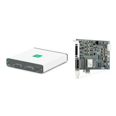
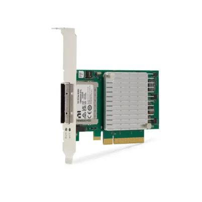
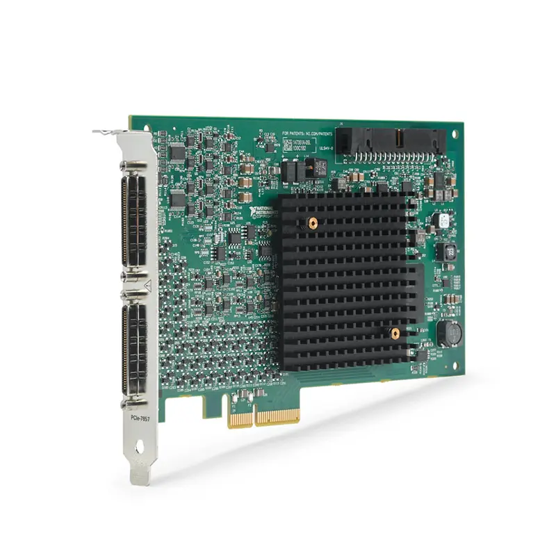
PCIe-7857 512 MB DRAM Multifunction Reconfigurable I/O Device
Земля PCIe-7857 is an R Series multifunction reconfigurable I/O device for PCI Express computers. It combines eight 16-bit analog inputs, eight 16-bit analog outputs, 48 bidirectional digital I/O lines, a Kintex-7 160T FPGA and 512 MB of onboard DRAM.
Each analog input has a dedicated analog-to-digital converter, allowing independent timing, individual channel triggering and multirate acquisition at up to 1 MS/s per channel. The eight analog outputs also support update rates up to 1 MS/s per channel.
The user-programmable FPGA provides direct hardware control over every I/O channel. This architecture supports deterministic applications such as hardware-in-the-loop testing, sensor simulation, custom protocol communication, waveform generation and high-speed closed-loop control.
Key Features of the PCIe-7857
- Eight 16-bit analog input channels
- Eight 16-bit analog output channels
- 48 bidirectional digital I/O channels
- 1 MS/s analog input rate per channel
- 1 MS/s analog output rate per channel
- Dedicated ADC for every analog input channel
- Simultaneous multichannel sampling
- Software-selectable ±1 V, ±2 V, ±5 V and ±10 V input ranges
- ±10 V analog output range
- Xilinx Kintex-7 160T FPGA
- 512 MB of onboard DRAM
- 800 MB/s DRAM streaming rate
- Up to 80 MHz digital I/O operation
- Multiple selectable digital logic families
- Sixteen DMA channels
- Eight RTSI synchronization lines
- Two 68-pin VHDCI I/O connectors
- PCI Express x4 host interface
- LabVIEW FPGA programming support
PCIe-7857 Technical Specifications
| Product Model | PCIe-7857 |
|---|---|
| Part Number | 786458-01 |
| Product Type | R Series multifunction reconfigurable I/O device with DRAM |
| ФПГА | Xilinx Kintex-7 160T |
| FPGA Flip-Flops | 202,800 |
| FPGA Lookup Tables | 101,400 |
| Embedded Block RAM | 11,700 kbits |
| DSP48 Slices | 600 |
| Onboard DRAM | 512 MB, one bank |
| Maximum DRAM Streaming Rate | 800 MB/s |
| Analog Input Channels | 8 |
| Analog Input Resolution | 16 bits |
| ADC Architecture | Dedicated successive-approximation ADC per channel |
| Analog Input Conversion Time | 1 мкс |
| Maximum Analog Input Rate | 1 Мвыб/с на канал |
| Analog Input Modes | Differential, NRSE and RSE |
| Analog Input Ranges | ±1 V, ±2 V, ±5 V and ±10 V |
| Analog Input Coupling | DC |
| Small-Signal Input Bandwidth | 1 MHz |
| Large-Signal Input Bandwidth | 500 kHz |
| Analog Input Absolute Accuracy | Approximately 2.28 mV at full scale under specified conditions |
| Analog Input Overvoltage Protection | ±42 V powered on; ±35 V powered off |
| Analog Output Channels | 8 |
| Analog Output Resolution | 16 bits |
| Analog Output Type | Single-ended voltage output |
| Analog Output Range | ±10 V |
| Maximum Analog Output Rate | 1 Мвыб/с на канал |
| Analog Output Coupling | DC |
| Analog Output Impedance | 0.5 Ω |
| Analog Output Current Drive | ±2.5 mA |
| Analog Output Slew Rate | 10 V/µs |
| Analog Output Protection | Short-circuit protection to ground |
| Digital I/O Channels | 48 bidirectional channels |
| Connector 0 Digital Channels | 16 channels, up to 10 MHz |
| Connector 1 Digital Channels | 32 channels, up to 80 MHz |
| Digital Logic Families | 1.2 V, 1.5 V, 1.8 V, 2.5 V and 3.3 V |
| Default Digital Logic Level | 3.3 V |
| Maximum Digital Output Current | 4 mA source or sink per channel |
| Minimum Digital Pulse Width | 6.25 ns |
| Minimum Digital Sampling Period | 5 ns |
| External Clock Maximum Frequency | 80 MHz |
| Selectable FPGA Timebases | 40 MHz, 80 MHz, 120 MHz, 160 MHz and 200 MHz |
| Default FPGA Timebase | 40 MHz |
| RTSI Resources | RTSI lines 0 through 7 |
| DMA Channels | 16 |
| Шинный интерфейс | PCI Express x4, specification 1.0 compliant |
| Compatible Slots | PCI Express x4, x8 and x16 |
| I/O Connectors | 2 × 68-pin VHDCI |
| Form Factor | Standard-height, half-length, single-slot PCI Express card |
| Board Dimensions | 16.8 cm × 11.1 cm |
PCIe-7857 Part Number and Accessories
| Item | Part Number | Описание |
|---|---|---|
| PCIe-7857 | 786458-01 | Kintex-7 multifunction reconfigurable I/O device with 512 MB DRAM |
| SCB-68A Connector Block | 782536-01 | Shielded, noise-rejecting connector block for multifunction analog and digital I/O |
| SCB-68 HSDIO Connector Block | 782914-01 | Shielded 68-pin connector block for R Series high-speed digital I/O |
| SHC68-68-RMIO Cable | 189588-01 | 1 m shielded cable for the multifunction I/O connector |
| SHC68-68-RMIO Cable | 189588-02 | 2 m shielded cable for the multifunction I/O connector |
| SHC68-C68-RDIO2 Cable | 156166-01 | 1 m shielded R Series high-speed digital I/O cable |
| SHC68-C68-RDIO2 Cable | 156166-02 | 2 m shielded R Series high-speed digital I/O cable |
| SHC68-NT-S Cable | 189041-02 | 2 m shielded VHDCI-to-unterminated cable for custom fixtures |
The multifunction and high-speed digital connectors use different cable configurations. Verify the required I/O channels, cable length, terminal-block type and test-fixture wiring before ordering accessories.
Kintex-7 160T FPGA Architecture
The PCIe-7857 contains a Xilinx Kintex-7 160T FPGA that directly controls its analog inputs, analog outputs, digital I/O, DMA channels and synchronization resources.
The FPGA can execute deterministic control and signal-processing logic independently of the host operating system. This avoids the variable timing associated with software-only I/O control.
FPGA Logic and DSP Resources
The FPGA provides 202,800 flip-flops, 101,400 lookup tables, 11,700 kbits of embedded block RAM and 600 DSP48 slices.
These resources can implement proportional-integral-derivative controllers, custom filters, protocol engines, trigger logic, waveform processing and other parallel hardware algorithms.
512 MB Onboard DRAM
The PCIe-7857 includes one 512 MB bank of onboard DRAM. This is its most important functional difference from the otherwise similar PCIe-7856.
Onboard DRAM allows the FPGA to store substantially larger data sets than can fit in embedded block RAM. It is useful for deep acquisition buffers, waveform playback, lookup tables and applications that temporarily produce data faster than the host can receive it.
800 MB/s DRAM Streaming
The onboard memory supports a maximum stated streaming rate of 800 MB/s. Actual throughput depends on memory-access patterns, FPGA logic, simultaneous operations and the selected data width.
Efficient burst transfers generally provide better DRAM performance than frequent small or irregular accesses. FPGA code should be designed around the characteristics of the external memory interface.
DRAM Waveform Storage
The 512 MB memory can hold long analog or digital waveform sequences that are later generated under deterministic FPGA timing. This reduces dependence on continuous host streaming.
Waveform data can be transferred to DRAM before a test begins, then accessed by the FPGA during high-speed stimulus generation or sensor simulation.
Deep Acquisition Buffering
High-speed analog or digital samples can be buffered in onboard DRAM before transfer to the host. This is useful for burst events and triggered acquisitions where preserving a long record is more important than immediately sending every sample to the computer.
The maximum record length depends on sample width, channel count and whether processed or raw data is stored.
Eight Dedicated Analog Input ADCs
Each analog input channel uses a dedicated 16-bit successive-approximation ADC. All eight channels can therefore acquire simultaneously without sharing a multiplexed converter.
The dedicated architecture supports multirate sampling and individual channel triggering. Separate channels can monitor signals with different timing requirements within one FPGA application.
1 MS/s Simultaneous Analog Input
Every input supports sampling at up to 1 MS/s. Because the rate applies per channel, all eight inputs can operate at their maximum rate simultaneously.
The FPGA can process samples as they arrive, transfer them through DMA or write them into the 512 MB onboard memory.
16-Bit Analog Input Resolution
The analog inputs provide 16-bit resolution across software-selectable bipolar ranges of ±1 V, ±2 V, ±5 V and ±10 V.
Using the smallest suitable range improves the nominal voltage represented by each ADC code. The selected range must still accommodate signal offset, noise and transient peaks.
Configurable Analog Input Modes
The inputs support differential, referenced single-ended and nonreferenced single-ended measurement modes. The selected mode applies to all analog input channels.
Differential mode provides improved common-mode noise rejection. RSE is appropriate for ground-referenced signals, while NRSE supports signals sharing a remote reference through AISENSE.
DC-Coupled Measurements
The analog inputs are DC coupled and can measure static voltages and time-varying signals. The stated small-signal bandwidth is 1 MHz, and the large-signal bandwidth is 500 kHz.
For precision measurements, use the recommended shielded cable and connector block and keep analog wiring separated from high-speed digital paths.
Analog Input Protection
The inputs provide overvoltage protection up to ±42 V with the device powered and ±35 V while powered off.
This protection helps with accidental connection faults but does not change the normal ±10 V maximum measurement range. Continuous signals should remain within the configured operating range.
Eight 16-Bit Analog Outputs
The PCIe-7857 provides eight independent analog voltage outputs with 16-bit resolution, a ±10 V range and a maximum update rate of 1 MS/s per channel.
FPGA-controlled output timing enables deterministic waveform generation, sensor simulation and closed-loop control.
Analog Output Drive Capability
Each analog output provides approximately 0.5 Ω output impedance and can source or sink up to 2.5 mA. The outputs include short-circuit protection to ground.
They are designed for high-impedance measurement and control inputs. Loads requiring additional current need a suitable external amplifier or buffer.
48 Bidirectional Digital I/O Channels
The PCIe-7857 includes 48 digital lines. Sixteen are available through the multifunction connector, and 32 higher-speed lines are available through the separate digital connector.
Each channel can be independently configured as an input or output in the FPGA design. Applications can implement triggers, pulse trains, digital buses and custom communication protocols.
Up to 80 MHz Digital Operation
The 32 channels on Connector 1 support frequencies up to 80 MHz. The 16 digital channels on Connector 0 support up to 10 MHz.
Use the SHC68-C68-RDIO2 cable and SCB-68 HSDIO connector block for high-speed digital signals. Cable length, loading and fixture layout can affect the attainable rate.
Selectable Digital Logic Levels
The digital I/O supports 1.2 V, 1.5 V, 1.8 V, 2.5 V and 3.3 V logic families. The voltage is selected per connector and defined during FPGA compilation.
The logic level cannot be changed dynamically while the compiled FPGA application is running. Verify external device compatibility before connecting the interface.
Sixteen DMA Channels
The PCIe-7857 provides 16 DMA channels for communication between the FPGA and host computer. Separate DMA FIFOs can transport acquisition data, generated waveforms, status information and control commands.
The onboard DRAM and DMA resources can work together: the FPGA can buffer a burst in DRAM and later transfer it to the host through a DMA FIFO.
RTSI Synchronization
RTSI lines 0 through 7 allow timing and triggers to be shared with compatible PCI and PCI Express devices in the same computer.
RTSI synchronization is useful when the PCIe-7857 must coordinate deterministic I/O with another data acquisition, counter/timer or R Series device.
Hardware-in-the-Loop Testing
The PCIe-7857 can acquire controller outputs, execute a simulation or control model and generate sensor signals with deterministic FPGA timing.
Its onboard DRAM is useful when long stimulus waveforms, fault sequences or acquired event records must be stored locally during the HIL test.
Sensor Simulation
The eight analog outputs can simulate voltage-based sensors, while the digital I/O can reproduce switches, pulse sensors and custom digital interfaces.
Large stimulus sequences can be stored in onboard DRAM and generated without relying on the host computer to supply every value in real time.
High-Speed Closed-Loop Control
The FPGA can acquire an analog signal, execute a control calculation and update an analog or digital output using predictable hardware timing.
Loop performance depends on ADC conversion time, FPGA calculation latency, DAC update time, analog settling and the connected plant.
Custom Protocol Communication
The reconfigurable digital lines can implement proprietary or application-specific protocols. FPGA logic can define clocks, framing, data encoding, handshaking and error detection.
External transceivers are required when the physical layer uses voltage or electrical standards not directly supported by the device’s LVCMOS I/O.
Typical PCIe-7857 Applications
- Hardware-in-the-loop testing
- Electronic control-unit validation
- Sensor and actuator simulation
- High-speed closed-loop control
- Deep triggered acquisition
- Onboard waveform storage and playback
- Custom digital protocol communication
- Multirate data acquisition
- Independent channel triggering
- Обработка сигналов на основе ПЛИС
- Power-electronics research
- Автоматизированное испытательное оборудование
- Production functional testing
- Real-time system prototyping
LabVIEW FPGA Programming
The PCIe-7857 is programmed using the LabVIEW FPGA Module. Developers create an FPGA VI defining the behavior of the analog inputs, analog outputs, digital I/O, memory and host interfaces.
The FPGA VI is compiled into a hardware bitfile for the Kintex-7 target. Compilation verifies resource use and whether the design can meet the selected clock timing.
R Series Software Support
The device requires compatible NI R Series Multifunction RIO drivers in addition to LabVIEW and LabVIEW FPGA. Host software communicates with the FPGA through controls, indicators, interrupts and DMA FIFOs.
Confirm the required LabVIEW and driver versions before integrating the PCIe-7857 into an existing development environment.
PCI Express Computer Integration
The device uses a PCI Express x4 interface compliant with PCI Express specification 1.0. It can be installed in compatible x4, x8 or x16 slots.
The board uses a standard-height, half-length, single-slot form factor. Check computer clearance, slot availability, cooling and cable access before installation.
PCIe-7857 Connection Architecture
Connector 0 carries the eight analog inputs, eight analog outputs, 16 digital I/O lines and reference connections. Connector 1 carries the 32 high-speed digital channels and external clock input.
Use the RMIO cable and SCB-68A for analog and multifunction signals. Use the RDIO2 cable and SCB-68 HSDIO for the high-speed digital interface.
PCIe-7857 Troubleshooting
The PCIe-7857 is not detected
Confirm that the device is fully installed in a compatible PCI Express slot. Check the R Series driver, operating-system support, computer firmware and Device Manager.
The FPGA design cannot access DRAM
Confirm that the project targets the PCIe-7857 rather than the PCIe-7856. Review the DRAM interface configuration, memory address range and example projects.
DRAM throughput is lower than expected
Use larger sequential burst transfers and reduce small random accesses. Check whether other FPGA processes or host transfers are competing for memory bandwidth.
Analog input readings are incorrect
Verify the input mode, range, pin assignment and reference connection. The differential, RSE or NRSE selection applies to all channels.
An analog input clips
Select a larger range or reduce the input signal. Include signal offset, common-mode voltage and transients when checking the range.
An analog output cannot drive the load
Check the load impedance and current requirement. Each output provides only ±2.5 mA and may require an external buffer for lower-impedance loads.
High-speed digital signals are unreliable
Use the recommended RDIO2 cable and HSDIO connector block. Verify digital voltage, cable length, termination, output loading and FPGA timing.
The digital voltage does not change at runtime
This is expected. Digital voltage is selected per connector during FPGA compilation and is not dynamically configurable.
DMA data is lost
Increase FIFO depth, service the host FIFO more frequently or buffer burst data in onboard DRAM before transferring it through DMA.
A PCIe-7856 FPGA project does not use the PCIe-7857 memory
Retarget the project to the PCIe-7857 and explicitly add DRAM operations. The similar I/O configuration does not automatically cause an existing FPGA design to use the added memory.
PCIe-7857 Comparison with Similar R Series Devices
| Модель | Primary Configuration | Best Suited For |
|---|---|---|
| PCIe-7857 | 8 AI, 8 AO, 48 DIO, Kintex-7 160T, 512 MB DRAM | Multifunction FPGA I/O requiring onboard waveform memory |
| PCIe-7856 | 8 AI, 8 AO, 48 DIO, Kintex-7 160T, no DRAM | Similar deterministic I/O without deep onboard memory |
| PCIe-7858 | 8 AI, 8 AO, 48 DIO, larger FPGA and onboard memory | More complex processing and large buffered applications |
| PCIe-7846 | 8 AI, 8 AO, 48 DIO, smaller FPGA | Applications with lower FPGA resource requirements |
| PXIe-7857 | 8 AI, 8 AO, 48 DIO, 512 MB DRAM, PXI Express | Equivalent functionality within a modular PXI system |
PCIe-7857 vs PCIe-7856
The PCIe-7857 and PCIe-7856 have the same principal analog, digital and FPGA configuration. Both provide eight analog inputs, eight analog outputs, 48 digital I/O lines and a Kintex-7 160T FPGA.
The PCIe-7857 adds 512 MB of onboard DRAM with an 800 MB/s streaming rate. Choose the PCIe-7857 for deep acquisition buffering, long waveform playback or FPGA algorithms requiring external memory. Choose the PCIe-7856 when onboard DRAM is unnecessary.
PCIe-7857 vs PCIe-7858
The PCIe-7858 is intended for applications requiring additional FPGA processing resources. The PCIe-7857 uses the Kintex-7 160T FPGA and is appropriate when its logic, DSP and memory capacity meet the design requirements.
Select the PCIe-7858 for more resource-intensive FPGA algorithms. Select the PCIe-7857 when 512 MB DRAM and the 160T FPGA provide sufficient capacity.
PCIe-7857 vs PXIe-7857
The PCIe-7857 installs in a PCI Express computer, while the PXIe-7857 installs in a PXI Express chassis. Their principal I/O, FPGA and DRAM capabilities are similar.
Choose the PCIe-7857 for workstation-based systems. Choose the PXIe-7857 when the application requires PXI chassis synchronization, modular instruments and peer-to-peer PXI data transfer.
Recommended Related Products
- PCIe-7856 Multifunction Reconfigurable I/O Device
- PCIe-7858 Multifunction Reconfigurable I/O Device
- PCIe-7846 Multifunction Reconfigurable I/O Device
- PXIe-7857 Multifunction Reconfigurable I/O Module with DRAM
- PXIe-7856 Multifunction Reconfigurable I/O Module
- USB-7856 Multifunction Reconfigurable I/O Device
- View More NI R Series Multifunction RIO Devices
- View More NI PCI and USB Data Acquisition Products
Selecting the Right R Series Device
Choose the PCIe-7857 when the application requires eight independently timed analog inputs, eight deterministic analog outputs, 48 reconfigurable digital channels and 512 MB of FPGA-accessible DRAM.
Select the PCIe-7856 when the same I/O and FPGA architecture is needed without external memory. Choose the PCIe-7858 for additional FPGA resources or the PXIe-7857 when the system must use the PXI Express platform.
Why Choose the PCIe-7857?
- Combines analog input, analog output and digital I/O
- Provides dedicated ADCs for simultaneous acquisition
- Samples eight analog channels at up to 1 MS/s each
- Generates eight independent 16-bit analog outputs
- Supports 48 bidirectional digital channels
- Provides up to 80 MHz digital operation
- Includes a programmable Kintex-7 160T FPGA
- Adds 512 MB of onboard DRAM
- Supports deep buffering and waveform playback
- Enables deterministic hardware-level control
- Provides 16 DMA channels for host communication
- Installs directly in a PCI Express computer
Frequently Asked Questions
What is the PCIe-7857?
The PCIe-7857 is an R Series multifunction reconfigurable I/O device with eight analog inputs, eight analog outputs, 48 digital I/O lines, a Kintex-7 160T FPGA and 512 MB DRAM.
What is the PCIe-7857 part number?
The standard NI part number is 786458-01.
How many analog inputs does it provide?
It provides eight 16-bit analog inputs. Each input has a dedicated ADC and can sample at up to 1 MS/s.
What analog input ranges are available?
The available software-selectable ranges are ±1 V, ±2 V, ±5 V and ±10 V.
How many analog outputs are available?
The device provides eight 16-bit analog outputs with a ±10 V range and a maximum update rate of 1 MS/s.
How many digital I/O channels does it provide?
It provides 48 bidirectional digital I/O lines: 16 on Connector 0 and 32 on Connector 1.
What is the maximum digital frequency?
The 32 digital lines on Connector 1 support up to 80 MHz. Connector 0 digital lines support up to 10 MHz.
Which FPGA does the PCIe-7857 use?
It uses a Xilinx Kintex-7 160T FPGA with 101,400 lookup tables, 600 DSP48 slices and 11,700 kbits of embedded block RAM.
How much onboard DRAM is included?
The PCIe-7857 includes one 512 MB DRAM bank with a maximum specified streaming rate of 800 MB/s.
What is the difference between PCIe-7857 and PCIe-7856?
The primary difference is memory. The PCIe-7857 includes 512 MB DRAM, while the PCIe-7856 does not include onboard DRAM.
Can every analog input use separate timing?
Yes. The dedicated ADCs and FPGA architecture support multirate acquisition and individual channel triggering.
Which digital logic levels are supported?
The supported logic families are 1.2 V, 1.5 V, 1.8 V, 2.5 V and 3.3 V.
Can digital voltage be changed at runtime?
No. Digital voltage is selected per connector and defined when the FPGA design is compiled.
Which cables are compatible?
Use an SHC68-68-RMIO cable for the multifunction connector and an SHC68-C68-RDIO2 cable for the high-speed digital connector.
Which PCI Express slots are supported?
The PCIe-7857 uses an x4 interface and can operate in compatible PCI Express x4, x8 or x16 slots.
Request a Quote for the PCIe-7857
Contact us for current availability, lead time and project pricing for the PCIe-7857 512 MB DRAM Multifunction Reconfigurable I/O Device. We can also help identify compatible RMIO and RDIO cables, SCB-68 connector blocks and related PCIe or PXIe R Series devices.















