






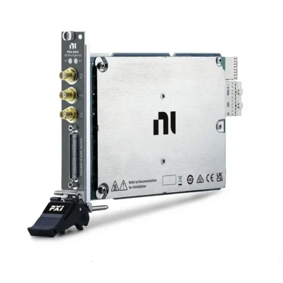
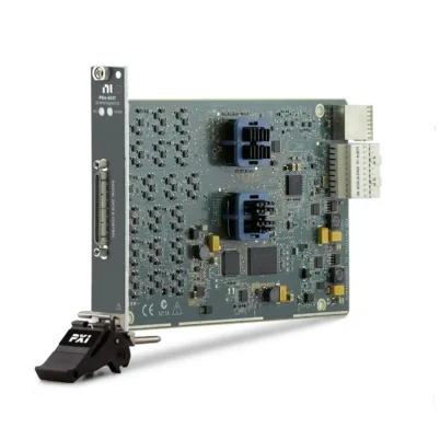
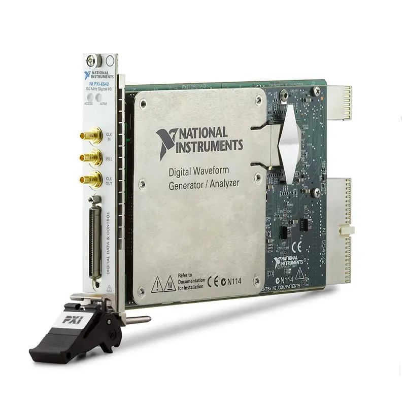
PXI-6542 32-Channel 100 MHz Digital Waveform Instrument
Земля PXI-6542 is a 32-channel PXI digital waveform generator and analyzer designed for functional testing, digital interface validation and mixed-signal test systems. Each single-ended digital channel can be configured independently for input or output operation.
The module generates and acquires digital patterns at rates up to 100 MHz. It supports selectable 1.8 V, 2.5 V and 3.3 V TTL logic families, with 3.3 V operation compatible with common 5 V TTL signal levels. Memory configurations of 1 Mbit, 8 Mbit or 64 Mbit per channel support applications with different waveform and record-length requirements.
Key Features of the PXI-6542
- 32 bidirectional single-ended digital data channels
- 100 MHz maximum sample clock
- Up to 100 Mbit/s SDR generation per channel
- Up to 100 Mbit/s SDR acquisition per channel
- Selectable 1.8 V, 2.5 V and 3.3 V logic families
- 5 V TTL-compatible operation in the 3.3 V setting
- Per-channel input or output direction control
- Four bidirectional programmable function interface lines
- Three clock-input terminals and two clock-output terminals
- Onboard and external sample-clock support
- PXI backplane clock and trigger synchronization
- 10 ps sample-clock delay adjustment resolution
- 1 Mbit, 8 Mbit or 64 Mbit memory per channel
- Scripted waveform generation
- Finite, continuous and multirecord acquisition
- 68-pin VHDCI digital data and control connector
- Front-panel SMB clock connections
- NI-HSDIO software support
PXI-6542 Technical Specifications
| Product Model | PXI-6542 |
|---|---|
| Product Type | PXI digital waveform generator/analyzer |
| Digital Data Channels | 32 bidirectional channels |
| Тип сигнала | Single-ended |
| Direction Control | Software-selectable per channel |
| Maximum Sample Clock | 100 MHz |
| Maximum Generation Rate | 100 Mbit/s per channel, SDR |
| Maximum Acquisition Rate | 100 Mbit/s per channel, SDR |
| Supported Logic Families | 1.8 V, 2.5 V and 3.3 V TTL |
| 5 V TTL Compatibility | Supported with the 3.3 V TTL logic-family setting |
| Output Impedance | 50 Ω nominal |
| Maximum 1.8 V Output Drive | ±8 mA |
| Maximum 2.5 V Output Drive | ±16 mA |
| Maximum 3.3 V Output Drive | ±32 mA |
| Data-Channel Power-On State | Drivers disabled with approximately 50 kΩ input impedance |
| Output Protection Range | 0 V to 5 V indefinitely |
| Input Impedance | 50 kΩ nominal |
| Input Protection Range | -1 V to 6 V |
| Programmable Function Interfaces | 4 bidirectional PFI channels |
| Clock Input Terminals | 3 |
| Clock Output Terminals | 2 |
| Onboard Clock Range | 48 Hz to 100 MHz |
| External Sample Clock Range | 20 kHz to 100 MHz for a compatible square-wave clock |
| Sample-Clock Sources | Onboard clock, CLK IN, PXI_STAR or STROBE for acquisition |
| Clock Delay Range | 0 to 1 sample-clock period |
| Clock Delay Resolution | 10 ps |
| Acquisition Data Delay Resolution | 1/256 of a sample-clock period |
| Typical Channel-to-Channel Skew | ±600 ps |
| Reference Clock | 10 MHz through PXI_CLK10 or front-panel CLK IN |
| Front Digital Connector | 68-pin VHDCI Digital Data and Control connector |
| Clock Connectors | SMB jacks |
| Typical Power Consumption | Approximately 15 W |
| Maximum Power Consumption | Approximately 20.5 W |
| Dimensions | 21.6 × 2.0 × 13.1 cm |
| Weight | Approximately 343 g |
| Поддержка программного обеспечения | NI-HSDIO |
| Lifecycle Status | Discontinued |
PXI-6542 Part Numbers and Memory Configurations
| Part Number | Memory per Channel | Total Onboard Memory | Описание |
|---|---|---|---|
| 778953-01 | 1 Mbit per channel | 4 MB total | Entry memory configuration for shorter generation and acquisition records |
| 778953-02 | 8 Mbit per channel | 32 MB total | Intermediate memory configuration for longer digital patterns |
| 778953-03 | 64 Mbit per channel | 256 MB total | Maximum memory configuration for long patterns and acquisition records |
The memory capacity is distributed across the 32 digital channels. Generation waveforms, scripts and acquisition records share the module’s Synchronization and Memory Core resources.
PXI-6542 Cables and Accessories
| Item | Part Number | Описание |
|---|---|---|
| SHC68-C68-D4 Cable | 781013-01 | 0.55 m shielded, 50 Ω, VHDCI-to-VHDCI digital cable |
| SHC68-C68-D4 Cable | 196275-01 | 1 m recommended shielded, 50 Ω digital cable |
| SHC68-C68-D4 Cable | 781293-01 | 2 m shielded digital cable |
| SHC68-C68-D4 Cable | 132625-03 | 3 m shielded cable with lower DC resistance |
| C68-C68-D4 Cable | 195949-01 | 1 m unshielded, 50 Ω digital cable |
| SHC68-H1X38 Cable | 192681-1R5 | 1.5 m shielded flying-lead cable for custom fixtures |
| CB-2162 | 778592-01 | Single-ended digital I/O connector block |
| SMB-2163 | 778747-01 | 32-channel rack-mountable SMB breakout accessory |
| SCB-68 HSDIO | 782914-01 | Shielded 68-pin HSDIO connector block |
| 653x Cable Adapter | 195846-01 | Adapter from 68-pin D-type accessories to the VHDCI cable interface |
NI specifies performance using a 1 m SHC68-C68-D4 shielded cable. Longer cables can increase reflections, timing uncertainty and signal degradation, so their performance may not meet the complete module specification.
32 Bidirectional Digital Channels
The PXI-6542 provides 32 single-ended digital data channels. Each channel can be configured independently as an input or output, allowing the module to work with interfaces that combine transmitted and received signals.
Unused output drivers can remain disabled to provide a high-impedance input state. This helps prevent electrical contention when the connected device controls the signal line.
Digital Waveform Generation
The module can generate user-defined digital patterns at rates up to 100 Mbit/s per channel. Each sample specifies the logic state of the configured output channels at one point in the hardware-timed sequence.
Generation applications include serial and parallel bus emulation, device initialization, protocol stimulus, memory-interface testing and digital control sequencing.
Digital Waveform Acquisition
The same digital channels can acquire input patterns at sample-clock rates up to 100 MHz. Captured data can be transferred to host memory or stored in onboard memory for later analysis.
Acquisition supports finite and continuous records, pretrigger samples and posttrigger samples. Multirecord operation allows several events to be captured without restarting the complete acquisition task.
100 MHz Sample Clock
The onboard sample clock covers a frequency range from approximately 48 Hz to 100 MHz. An external sample clock can also be supplied through the front-panel CLK IN connector.
At 100 MHz, the sample period is 10 ns. Cable delay, setup time, hold time and signal integrity must all be considered when interfacing with a device under test at the maximum rate.
Selectable Logic Families
The PXI-6542 supports standardized 1.8 V, 2.5 V and 3.3 V logic-family settings. The selected family configures the output voltage, input thresholds and available output drive strength.
Unlike digital instruments with continuously programmable voltage thresholds, the PXI-6542 uses predefined logic families. Confirm that the device under test is compatible with one of these supported settings.
5 V TTL Compatibility
The 3.3 V TTL setting is designed to interface with common 5 V TTL-compatible inputs and outputs. The PXI-6542 output high level is not a 5 V CMOS level.
A 5 V CMOS device may require a higher high-level input voltage than the module can generate. Review the device-under-test VIH and VOH specifications before connection.
Output Drive Strength
Maximum DC drive strength depends on the selected logic family. The documented values are approximately ±8 mA at 1.8 V, ±16 mA at 2.5 V and ±32 mA at 3.3 V.
These values are signal-drive ratings and should not be interpreted as power-output capability. Large capacitive loads and multiple unterminated branches can degrade edge quality.
Per-Channel Direction Control
Direction is configured independently for each of the 32 data channels. This supports interfaces in which some lines are always outputs, some are inputs and others change direction during a test.
The application must coordinate direction changes with the device under test to prevent both devices from driving a line at the same time.
Safe Power-On State
At power-up, the data-channel output drivers are disabled. Each channel presents an input impedance of approximately 50 kΩ until software explicitly enables generation.
This default state reduces the risk of driving an unknown value into a connected device during system startup. The test program should establish device-under-test power and signal direction before enabling outputs.
Synchronization and Memory Core
The PXI-6542 uses NI Synchronization and Memory Core architecture. Waveform samples, acquisition data and generation-script instructions share flexible onboard memory resources.
This architecture allows users to trade waveform count, record length and script complexity according to application requirements instead of using fixed memory partitions.
Scripted Pattern Generation
Scripted generation can execute a sequence of stored digital waveforms. Scripts support repeated patterns, conditional branches and trigger-controlled progression through a test sequence.
A waveform can be generated once, a defined number of times or continuously. Finite repeat counts can extend to more than 16 million repetitions.
Pattern Regeneration
Stored waveforms can be regenerated directly from onboard memory without retransmitting every sample from the host. This reduces PXI bus traffic and improves timing repeatability for periodic patterns.
Long nonrepeating patterns may be streamed from the controller if the complete system sustains the required transfer rate.
Multirecord Acquisition
Multirecord mode captures several separate events into onboard memory. Each record can include samples acquired before and after a reference trigger.
This mode is useful for intermittent bus transactions, packet capture and repeated device events separated by periods that do not need to be recorded.
Programmable Sample Timing
The sample-clock timing can be shifted over one complete clock period with adjustment resolution as fine as 10 ps. Acquisition data delay can also be adjusted in increments of 1/256 of a sample-clock period.
Timing adjustment helps position generation edges and acquisition sample points relative to the device-under-test timing window.
Setup and Hold Optimization
Moving the acquisition sampling point can compensate for cable delay and center the sample within the stable portion of the data eye. This improves reliability when testing interfaces near their timing limits.
Timing adjustment cannot correct severe signal-integrity problems. Proper impedance control, termination, grounding and cable selection remain essential.
Four PFI Channels
Four programmable function interface channels support triggers, events and additional application-specific control signals. Direction is configurable independently for each PFI line.
PFI lines can coordinate the digital pattern with a device-under-test ready signal, external event or another instrument.
External Sample Clock
A sample clock can be supplied through the front-panel SMB CLK IN connector. Compatible square-wave clock frequencies extend from approximately 20 kHz to 100 MHz.
The input is AC-coupled and offers software-selectable 50 Ω or 1 kΩ impedance. The clock must be continuous and satisfy the specified amplitude and duty-cycle limits.
STROBE-Based Acquisition
The STROBE terminal on the digital data and control connector can serve as the acquisition sample clock. This enables source-synchronous capture in which the device under test provides a clock alongside the data.
Source-synchronous operation helps preserve timing relationships when data and clock experience similar propagation delay through the cable and fixture.
Reference Clock and PLL
The PXI-6542 can lock its internal timing circuitry to the PXI 10 MHz backplane clock or an external 10 MHz reference connected to CLK IN.
Reference-clock synchronization allows multiple digital and mixed-signal instruments to share a common frequency reference. The documented PLL lock time is approximately 400 ms.
PXI_STAR Synchronization
PXI_STAR can be used as a sample-clock or trigger source. It supports start, reference, advance, pause and script-trigger functions according to the selected acquisition or generation mode.
Using the PXI backplane reduces the need for external synchronization cables and helps build tightly integrated mixed-signal test systems.
Typical PXI-6542 Applications
- Digital interface functional testing
- Parallel bus generation and acquisition
- Memory-interface validation
- ASIC and FPGA functional testing
- Embedded controller validation
- Digital protocol emulation
- Production electronic testing
- Mixed-signal stimulus-response systems
- Device initialization and configuration
- Digital sensor simulation
- Hardware-in-the-loop testing
- Timing margin characterization
- Автоматизированное испытательное оборудование
FPGA and ASIC Functional Testing
The PXI-6542 can apply known input vectors to an FPGA or ASIC and capture its digital response. Test software can compare acquired patterns with expected results to verify device behavior.
The module does not provide the per-pin parametric measurement and advanced hardware compare capabilities of a dedicated digital pattern instrument. External measurement hardware may be required for leakage and voltage-current characterization.
Parallel Bus Testing
Thirty-two data channels can emulate or monitor parallel digital buses. Additional PFI, STROBE and clock terminals support handshaking and source-synchronous timing.
Custom protocols can be implemented through waveform data and scripts without requiring a protocol-specific communications instrument.
Mixed-Signal Test Systems
The module can synchronize with digitizers, waveform generators, power supplies and other PXI instruments through shared reference clocks and triggers.
A mixed-signal test can apply analog and digital stimulus while acquiring the corresponding analog and digital response within a coordinated timing sequence.
Production Test Systems
In production testing, stored pattern sequences can validate digital assemblies without repeatedly transferring every vector from the host. Memory size should be selected according to test-pattern length and required acquisition history.
Reusable scripts can improve test throughput by executing loops and trigger-controlled sequences directly on the instrument.
NI-HSDIO Software Support
The PXI-6542 is controlled through the NI-HSDIO driver. NI-HSDIO provides APIs for channel configuration, waveform generation, acquisition, memory management, scripting, triggering, timing and synchronization.
The driver integrates with LabVIEW, LabWindows/CVI and compatible text-based development environments. Driver and operating-system compatibility should be verified because the PXI-6542 is a discontinued instrument.
Signal Integrity and Termination
The data interface and recommended cables use a nominal 50 Ω environment. Proper termination reduces reflections, overshoot, undershoot and false transitions.
Keep stubs short, avoid unnecessary adapters and use controlled-impedance fixture traces. The correct termination arrangement depends on source impedance, load impedance, cable length and signal direction.
PXI-6542 Lifecycle Status
The PXI-6542 is discontinued and is no longer available directly from NI. It may remain suitable for maintaining existing systems whose test vectors, cabling and NI-HSDIO software were developed around this instrument.
For new systems, consider the PXIe-6544 for similar 32-channel, 100 MHz functionality with additional low-voltage logic-family support and a PXI Express interface.
PXI-6542 Troubleshooting
The PXI-6542 is not detected
Confirm that the module is fully inserted into a compatible PXI or PXI hybrid slot. Check chassis power, controller communication and NI-HSDIO installation, then restart the system.
Generated outputs remain in a high-impedance state
Verify that the channels are configured for generation and that the output drivers have been enabled. The default power-on state leaves all drivers disabled.
The device under test does not recognize logic high
Confirm the selected logic family and the device-under-test VIH requirement. A 3.3 V TTL output may be compatible with 5 V TTL but not with every 5 V CMOS input.
Acquired data contains intermittent bit errors
Check termination, grounding, cable length and signal amplitude. Adjust the acquisition data delay to place the sample point within the stable timing window.
The module cannot acquire at 100 MHz
Verify the clock amplitude, duty cycle and continuity. Use the recommended 1 m cable and ensure that the data satisfies the required setup and hold times.
The external clock is not detected
Confirm that CLK IN is selected and configured for the correct impedance. Verify clock amplitude, frequency and duty cycle against the official input specifications.
Continuous generation stops unexpectedly
Check for a waveform-buffer underflow. Use onboard regeneration for repeating patterns or increase host buffering and transfer efficiency for streaming generation.
The acquired record does not include the expected event
Review the start and reference trigger sources, trigger polarity, pretrigger sample count and record length. Confirm that the trigger terminal is correctly routed.
Channels become hot during operation
The PXI-6542 can reach high operating temperatures. Maintain the required chassis airflow and allow the module to cool before removal.
An accessory does not connect to the VHDCI cable
Confirm whether the accessory uses a VHDCI or 68-pin D-type connector. A 653x cable adapter may be required for compatible D-type accessories.
PXI-6542 Comparison with Similar Digital Instruments
| Модель | Каналы | Maximum Rate | Logic-Level Capability | Best Suited For |
|---|---|---|---|---|
| PXI-6541 | 32 | 50 MHz | Selectable standard logic families | Lower-speed legacy digital waveform testing |
| PXI-6542 | 32 | 100 MHz | 1.8 V, 2.5 V and 3.3 V TTL | Legacy 100 MHz digital generation and acquisition |
| PXI-6552 | 20 | 100 MHz | Programmable voltage levels | Testing that requires adjustable thresholds and hardware comparison |
| PXIe-6544 | 32 | 100 MHz | 1.2 V, 1.5 V, 1.8 V, 2.5 V and 3.3 V | Modern PXI Express replacement for standard digital waveform testing |
| PXIe-6545 | 32 | 200 МГц | Selectable standard logic families | Higher-speed PXI Express digital waveform testing |
| PXIe-6547 | 32 | 100 MHz SDR, 200 Mbit/s DDR | Programmable from 1.2 V to 3.3 V | Adjustable voltage levels and hardware comparison |
PXI-6542 vs PXI-6541
Земля PXI-6541 and PXI-6542 both provide 32 bidirectional single-ended channels and similar memory options. The PXI-6541 operates at up to 50 MHz, while the PXI-6542 doubles the maximum rate to 100 MHz.
Choose the PXI-6542 when the digital interface requires rates above 50 MHz. The PXI-6541 may be sufficient for slower legacy test systems.
PXI-6542 vs PXI-6552
Земля PXI-6552 provides fewer digital data channels but adds programmable voltage levels and hardware comparison capabilities. Both instruments support rates up to 100 MHz.
Select the PXI-6542 for 32-channel density and standard logic families. Select the PXI-6552 when adjustable thresholds and onboard comparison are more important than channel count.
PXI-6542 vs PXIe-6544
Земля PXIe-6544 provides 32 channels and a 100 MHz maximum rate in a modern PXI Express format. It also adds support for 1.2 V and 1.5 V logic families.
The PXIe-6544 is generally preferable for a new system. The PXI-6542 remains useful when maintaining a legacy PXI platform and existing NI-HSDIO application.
PXI-6542 vs PXIe-6547
Земля PXIe-6547 provides 32 channels, programmable voltage levels from 1.2 V to 3.3 V, DDR operation and hardware comparison.
Choose the PXIe-6547 for broader voltage flexibility and more advanced functional testing. Choose the PXI-6542 when compatibility with an existing standard-logic PXI test system is required.
Recommended Related Products
- PXI-6541 32-Channel Digital Waveform Instrument
- PXI-6552 Programmable-Voltage Digital Waveform Instrument
- PXIe-6544 32-Channel 100 MHz Digital Waveform Instrument
- PXIe-6545 32-Channel 200 MHz Digital Waveform Instrument
- PXIe-6547 Programmable-Voltage Digital Waveform Instrument
- PXIe-6548 200 MHz Digital Waveform Instrument
- PXIe-6537 High-Speed Digital I/O Module
- View More NI PXI and PXI Express Modules
Selecting the Right Digital Waveform Instrument
Choose the PXI-6542 when maintaining an existing PXI system that requires 32 bidirectional channels, 100 MHz acquisition and generation, selectable standard logic families and NI-HSDIO compatibility.
Select the PXI-6552 when programmable voltage thresholds are required. For a new PXI Express system, consider the PXIe-6544, PXIe-6547 or PXIe-6548 according to rate, voltage and hardware-comparison requirements.
Why Choose the PXI-6542?
- Provides 32 independently configurable digital channels
- Generates and acquires patterns at up to 100 MHz
- Supports common 1.8 V, 2.5 V and 3.3 V logic
- Interfaces with compatible 5 V TTL devices
- Offers three onboard memory configurations
- Supports scripted waveform generation
- Provides multirecord triggered acquisition
- Includes fine generation and acquisition timing adjustment
- Supports external and source-synchronous clocks
- Synchronizes with mixed-signal PXI instruments
- Integrates with NI-HSDIO software
Frequently Asked Questions
What is the PXI-6542?
The PXI-6542 is a 32-channel, 100 MHz PXI digital waveform generator and analyzer for functional testing of single-ended digital interfaces.
What are the PXI-6542 part numbers?
Part number 778953-01 provides 1 Mbit per channel, 778953-02 provides 8 Mbit per channel and 778953-03 provides 64 Mbit per channel.
How many digital channels does the PXI-6542 provide?
It provides 32 bidirectional digital data channels with direction control on each channel.
What is the maximum data rate?
The module generates and acquires single-data-rate digital waveforms at up to 100 Mbit/s per channel using a 100 MHz sample clock.
Which logic levels are supported?
The PXI-6542 supports selectable 1.8 V, 2.5 V and 3.3 V TTL logic families. The 3.3 V setting is compatible with common 5 V TTL levels.
Does the PXI-6542 provide programmable voltage thresholds?
No. It provides predefined logic-family settings. Consider the PXI-6552 or PXIe-6547 when adjustable voltage levels and thresholds are required.
Can each channel be configured independently?
Yes. Each digital data channel can be configured independently for input or output operation.
Does the PXI-6542 support an external sample clock?
Yes. A compatible external sample clock can be supplied through the front-panel CLK IN SMB connector or through the STROBE terminal for source-synchronous acquisition.
Does the PXI-6542 perform hardware comparison?
It is primarily a digital generator/analyzer and does not provide the advanced hardware-comparison capabilities available on models such as the PXI-6552 and PXIe-6547.
Which cable is recommended?
NI recommends a 1 m SHC68-C68-D4 shielded 50 Ω cable, part number 196275-01, for specified performance.
Which breakout accessory provides individual SMB connectors?
The SMB-2163, part number 778747-01, provides individual SMB connections for the digital channels, clock and PFI signals.
Which software controls the PXI-6542?
The PXI-6542 is controlled through the NI-HSDIO driver and can be integrated with LabVIEW, LabWindows/CVI and compatible programming environments.
Is the PXI-6542 discontinued?
Yes. The PXI-6542 is discontinued and is primarily used for maintaining established digital and mixed-signal PXI test systems.
Request a Quote for the PXI-6542
Contact us for current availability, condition, memory configuration, lead time and project pricing for the PXI-6542 32-Channel 100 MHz Digital Waveform Instrument. Please specify whether you require the 1 Mbit, 8 Mbit or 64 Mbit-per-channel version. We can also help identify compatible VHDCI cables, connector blocks and newer PXI Express digital instruments.















