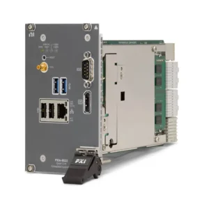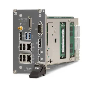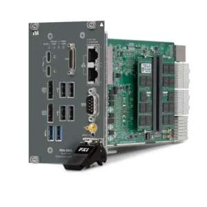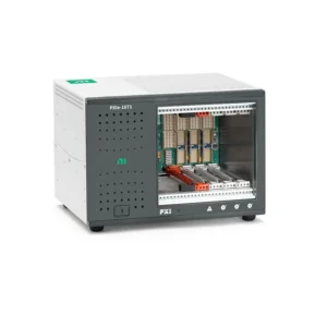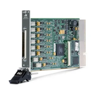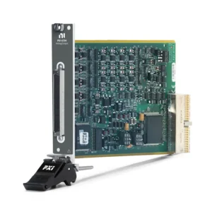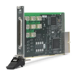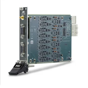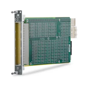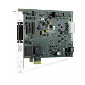


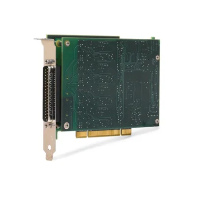
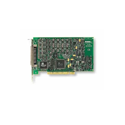
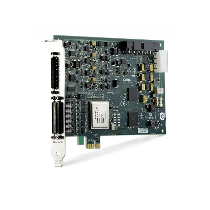
PCIe-7851R FPGA-Based R Series Multifunction RIO Device
Земля PCIe-7851R, also commonly identified as the PCIe-7851, is an NI R Series multifunction reconfigurable I/O device designed for hardware-in-the-loop testing, high-speed control, custom digital protocols and onboard signal processing.
The device combines eight independent 16-bit analog inputs, eight independent 16-bit analog outputs and 96 individually configurable digital I/O lines with a user-programmable Xilinx Virtex-5 LX30 FPGA.
Unlike a conventional multifunction DAQ board with a fixed hardware personality, the PCIe-7851R allows engineers to program its FPGA using the LabVIEW FPGA Module. Timing, triggering, signal processing, control logic and custom communication functions can run directly on the device with deterministic hardware execution.
Key Features of the PCIe-7851R
- Xilinx Virtex-5 LX30 user-programmable FPGA
- Eight independent analog input channels
- 16-bit analog input resolution
- 750 kS/s maximum analog input rate per channel
- Simultaneous analog input sampling
- Eight independent 16-bit analog outputs
- Up to 1 MS/s analog output update rate
- 96 individually configurable digital I/O lines
- Up to 40 MHz digital I/O operation
- Hardware-timed control and signal processing
- Custom triggering and timing logic
- PCI Express host interface
- LabVIEW FPGA and NI-RIO software support
PCIe-7851R Technical Specifications
| Product Model | PCIe-7851R / PCIe-7851 |
|---|---|
| Part Number | 781102-01 |
| Product Type | R Series Multifunction Reconfigurable I/O Device |
| Шинный интерфейс | PCI Express |
| ФПГА | Xilinx Virtex-5 LX30 |
| Analog Input Channels | 8 independent channels |
| Analog Input Resolution | 16 bits |
| Maximum AI Sample Rate | 750 kS/s per channel |
| Simultaneous Sampling | Да |
| Analog Input Range | Software-selectable bipolar voltage ranges up to ±10 V |
| Analog Output Channels | 8 independent channels |
| Analog Output Resolution | 16 bits |
| Maximum AO Update Rate | 1 Мвыб/с на канал |
| Analog Output Range | Up to ±10 V |
| Цифровой ввод-вывод | 96 bidirectional lines |
| Digital I/O Rate | Up to 40 MHz |
| Digital Logic | 3.3 V TTL compatible |
| FPGA Programming | LabVIEW FPGA Module |
| Device Driver | NI-RIO |
| Front Connections | High-density VHDCI connectors |
PCIe-7851R Part Number and Accessories
| Item | Part Number or Type | Описание |
|---|---|---|
| PCIe-7851R | 781102-01 | Virtex-5 LX30 FPGA R Series device with 8 AI, 8 AO and 96 DIO |
| SHC68-C68-RDIO2 | Shielded VHDCI cable | Connects R Series digital I/O to a compatible terminal accessory |
| SHC68-68-RMIO | Shielded multifunction cable | Provides access to compatible analog and digital I/O connections |
| SCB-68 Series | Shielded connector block | Provides screw-terminal access for custom test-system wiring |
| LabVIEW FPGA Module | Development software | Used to compile custom FPGA logic for the PCIe-7851R |
The PCIe-7851R uses multiple high-density connectors for its analog and digital resources. Verify the connector number, cable type and terminal accessory required for each I/O bank before ordering.
Virtex-5 LX30 FPGA Architecture
The onboard FPGA gives the PCIe-7851R a reconfigurable hardware personality. Engineers can implement custom trigger logic, pulse generation, signal processing, safety interlocks and digital communication directly in hardware.
FPGA code executes independently of the nondeterministic timing of a desktop operating system. This makes the device useful when an application requires repeatable microsecond-level or submicrosecond-level responses.
Eight Simultaneous Analog Inputs
The device includes eight independent 16-bit analog inputs with one ADC per channel. All eight channels can sample simultaneously, preserving phase and timing relationships between signals.
Independent conversion is valuable for multiaxis control, power-electronics testing, motor control and hardware-in-the-loop applications involving several synchronized feedback signals.
Eight Hardware-Timed Analog Outputs
Eight 16-bit analog outputs can generate control signals, sensor simulations and voltage stimuli. FPGA logic can update the outputs in direct response to acquired signals or digital events.
The analog outputs are signal-level outputs. External amplification, isolation or current drivers may be required when controlling motors, valves or other power loads.
96 Reconfigurable Digital I/O Lines
Every digital line can be configured as an input or output through the FPGA application. The large channel count supports custom parallel buses, digital pattern generation, state monitoring and high-speed device control.
The FPGA can also implement nonstandard communication protocols that are not available from conventional serial or industrial interface devices.
Hardware-in-the-Loop Testing
The PCIe-7851R can simulate sensors, read controller outputs and execute control models with deterministic timing. FPGA-based logic can respond to DUT activity without waiting for a Windows software loop.
For example, analog outputs can simulate sensor voltages while analog inputs measure actuator feedback and digital lines reproduce switches, encoders or communication states.
Custom FPGA Signal Processing
Filtering, scaling, threshold detection, pulse analysis and control calculations can run on the FPGA before data is transferred to the host computer.
Onboard processing can reduce PCI Express bandwidth and improve response time because the device sends only the data or events required by the host application.
PCIe-7851R Applications
- Hardware-in-the-loop testing
- Rapid control prototyping
- Motor and power-electronics control
- Custom digital communication protocols
- Sensor and actuator simulation
- Высокоскоростное управление станком
- Обработка сигналов на основе ПЛИС
- Automotive ECU validation
- Aerospace controller testing
- Deterministic safety interlocks
- Multiaxis control systems
- Automated electronic testing
PCIe-7851R Installation Workflow
Step 1: Verify PCI Express Compatibility
Confirm that the computer provides a compatible PCI Express slot and sufficient internal clearance and cooling.
Step 2: Install the Software
Install compatible versions of LabVIEW, the LabVIEW FPGA Module and the NI-RIO driver before configuring the target.
Step 3: Install the PCIe-7851R
Power down the computer, observe ESD precautions, insert the device fully into the PCI Express slot and secure its mounting bracket.
Step 4: Connect the I/O Accessories
Attach the correct shielded VHDCI cables and terminal accessories. Match each cable to the appropriate connector and I/O bank.
Step 5: Add the FPGA Target
Add the PCIe-7851R to the LabVIEW project and verify that the FPGA target is detected correctly.
Step 6: Compile and Download the FPGA VI
Compile the FPGA application for the Virtex-5 LX30 target, download the resulting bitfile and test the I/O at safe signal levels.
PCIe-7851R Troubleshooting
The device is not detected
Check PCI Express seating, NI-RIO installation, Device Manager and software compatibility. Confirm that the selected slot supports the installed board.
The FPGA VI cannot compile
Verify the selected FPGA target, LabVIEW FPGA version and device support. Reduce resource usage if the design exceeds the LX30 FPGA capacity.
Analog readings contain noise
Check grounding, shielding, input range and cable routing. Keep sensitive analog connections separated from rapidly switching digital lines and power conductors.
Digital I/O does not change state
Confirm that the FPGA VI configures the line for the intended direction and that external voltage levels are compatible with the device.
The host cannot keep up with acquired data
Use DMA FIFOs, reduce unnecessary data transfers or perform filtering and decimation on the FPGA before sending data to the computer.
PCIe-7851R Comparison
| Модель | ФПГА | Analog I/O | Цифровой ввод-вывод | Primary Difference |
|---|---|---|---|---|
| PCIe-7851R | Virtex-5 LX30 | 8 AI / 8 AO | 96 | Entry Virtex-5 785xR FPGA size |
| PCIe-7852R | Virtex-5 LX50 | 8 AI / 8 AO | 96 | Additional FPGA resources |
| PCIe-7856 | Newer FPGA generation | 8 AI / 8 AO | 48 | Higher analog performance |
| PCIe-7857 | Newer, larger FPGA | 8 AI / 8 AO | 48 | More FPGA resources |
PCIe-7851R vs Conventional DAQ
A conventional DAQ device has predetermined acquisition, output and timing functions. The PCIe-7851R allows these functions to be redesigned through FPGA programming, making it more suitable for custom and deterministic applications.
Frequently Asked Questions
Are PCIe-7851 and PCIe-7851R the same product?
The official NI model is PCIe-7851R. PCIe-7851 is commonly used as a shortened search and inventory name.
Which FPGA does the PCIe-7851R use?
It uses a Xilinx Virtex-5 LX30 FPGA.
How many analog channels are available?
The device provides eight 16-bit analog inputs and eight 16-bit analog outputs.
How many digital I/O lines are available?
It provides 96 individually configurable digital I/O lines.
Does the PCIe-7851R require LabVIEW FPGA?
LabVIEW FPGA is required to develop and compile custom FPGA applications. A previously compiled bitfile can be deployed without recompiling it.
Recommended Related Products
- PCIe-7852R Multifunction RIO Device
- PCIe-7856 FPGA Multifunction I/O Device
- PCIe-7857 FPGA Multifunction I/O Device
- USB-7855R Multifunction RIO Device
- View More NI Data Acquisition Hardware
Request a Quote for the PCIe-7851R
Contact us for current availability, condition and pricing for the PCIe-7851R FPGA-based multifunction RIO device. We can also help identify compatible VHDCI cables, terminal accessories and alternative NI FPGA hardware.