






Product Introduction
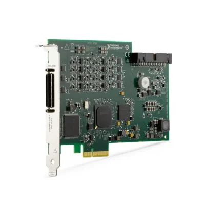
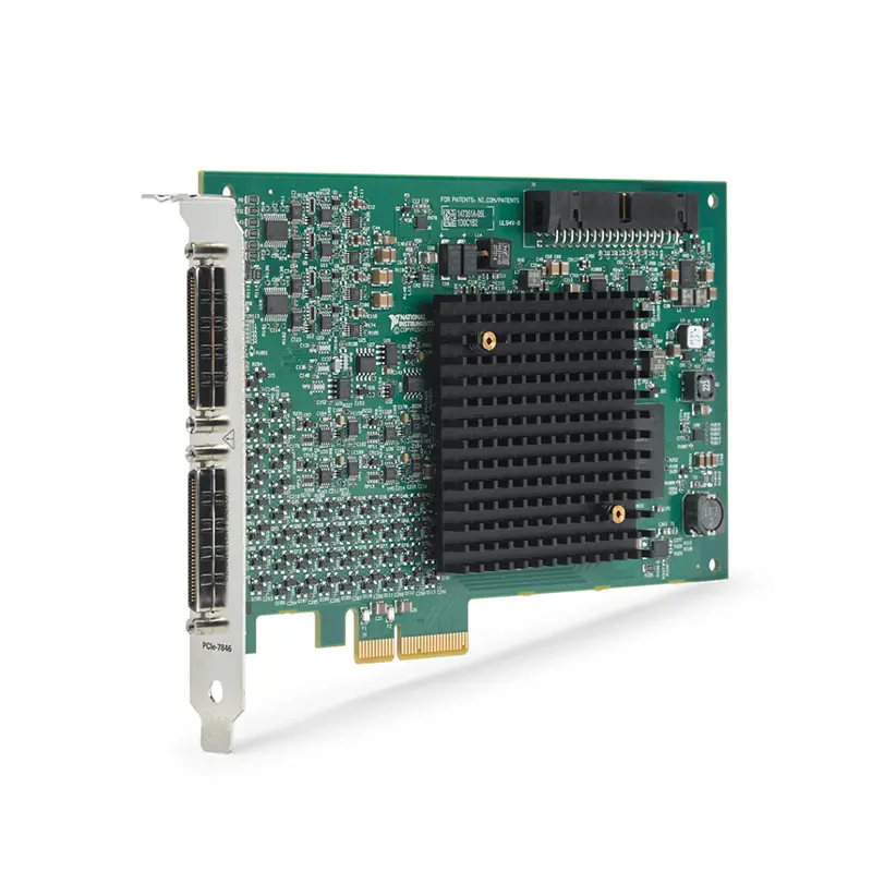
Земля NI PCIe-7846 высокопроизводительный R Series Multifunction Reconfigurable I/O (RIO) device designed for hardware-in-the-loop (HIL) testing, sensor simulation, custom protocol communication, high-speed control, automated test, and FPGA-based measurement applications.
The PCIe-7846 combines multifunction analog and digital I/O with a user-programmable Xilinx Kintex-7 160T FPGA. Unlike conventional multifunction DAQ devices that rely primarily on host software for processing and timing, the PCIe-7846 allows engineers to implement custom hardware logic directly on the FPGA for deterministic timing, triggering, signal processing, and control.
With a maximum analog input sample rate of 500 kS/s, dedicated analog-to-digital conversion resources, 48 bidirectional digital I/O channels, and a PCI Express host interface, the PCIe-7846 is well suited for demanding embedded test and control applications.
Product Overview
Земля National Instruments PCIe-7846 belongs to the NI R Series Multifunction RIO family.
A typical system architecture is:
Sensors / DUT / Digital Signals → PCIe-7846 I/O → Kintex-7 FPGA → PCI Express → Host Computer
The onboard FPGA can execute custom logic independently of the host operating system, providing deterministic response for applications where microsecond-level or hardware-timed behavior is required.
Key Features
FPGA Kintex-7 160T
The PCIe-7846 incorporates a Xilinx Kintex-7 160T FPGA for user-defined hardware processing.
The FPGA can be programmed to implement application-specific functions such as:
- Custom hardware triggering
- High-speed control loops
- Digital protocol implementation
- Signal processing
- Sensor simulation
- Custom timing engines
- Event detection
- Interlock logic
- Data reduction
- Hardware-in-the-loop interfaces
500 kS/s Analog Input Sampling
The PCIe-7846 supports analog input sampling rates up to 500 kS/s.
This acquisition performance makes the device suitable for control, simulation, automated test, and dynamic measurement applications that require faster deterministic acquisition than conventional low-speed control hardware.
Dedicated ADC per Analog Input Channel
A key advantage of the PCIe-7846 is its dedicated analog-to-digital converter architecture.
Instead of multiplexing several analog channels through a single ADC, dedicated conversion resources enable independent channel timing and triggering.
This architecture supports advanced functions such as:
- Independent channel triggering
- Multirate sampling
- Deterministic acquisition
- Channel-specific timing
- Parallel measurement processing
Multirate Sampling
The FPGA-based architecture enables multirate sampling, allowing different measurement and control operations to execute according to application-specific timing requirements.
For example, one group of signals can be acquired at a high rate while another control or monitoring function operates at a lower rate.
Individual Channel Triggering
The PCIe-7846 supports application architectures where individual analog channels can use independent triggering behavior.
This capability provides substantially greater flexibility than conventional multifunction DAQ hardware when different signals require different acquisition conditions.
48 Bidirectional Digital I/O Channels
The PCIe-7846 provides 48 bidirectional digital I/O channels.
The digital I/O can be controlled directly from FPGA logic for deterministic digital communication, control, monitoring, and protocol implementation.
Области применения включают:
- DUT control
- Digital status monitoring
- Custom protocol communication
- Trigger generation
- Hardware interlocks
- Генерация импульсов
- Sensor simulation
- Digital test interfaces
Up to 80 MHz Clock Rate
The PCIe-7846 provides a maximum digital clock rate of up to 80 MHz, enabling high-speed FPGA-controlled digital operations for compatible applications.
PCI Express Interface
The PCIe-7846 installs directly into a compatible PCI Express slot in a desktop, workstation, industrial computer, or automated test platform.
The PCI Express interface provides high-speed communication between the FPGA-based R Series device and the host computer.
Deterministic FPGA Processing
One of the primary advantages of the PCIe-7846 is that critical measurement and control functions can execute directly in FPGA hardware rather than depending entirely on the host operating system.
A typical architecture is:
Input Signal → FPGA Processing → Decision Logic → Output Response
This architecture is valuable for applications requiring predictable and repeatable timing.
Technical Specifications
| Параметр | Спецификация |
|---|---|
| Product Type | R Series Multifunction Reconfigurable I/O Device |
| Модель | PCIe-7846 |
| Manufacturer | Национальные инструменты |
| Part Number | 786456-01 |
| Шинный интерфейс | PCI Express |
| Maximum Analog Input Sample Rate | 500 kS/s |
| ADC Architecture | Dedicated ADC per Analog Input Channel |
| ФПГА | Xilinx Kintex-7 160T |
| Bidirectional Digital I/O | 48 Channels |
| Maximum Clock Rate | 80 MHz |
| FPGA Programmable | Да |
| Multirate Sampling | Supported |
| Individual Channel Triggering | Supported |
| Primary Programming Environment | LabVIEW FPGA Module |
| Primary Applications | HIL Testing, Sensor Simulation, Custom Protocols, High-Speed Control and Automated Test |
How Does the PCIe-7846 Work?
The PCIe-7846 combines analog and digital I/O with a user-programmable FPGA.
A simplified signal path is:
Physical Signal → Analog / Digital I/O → Kintex-7 FPGA → Custom Processing → PCI Express → Host Application
For output or control applications, the FPGA can also respond directly to acquired signals:
Input → FPGA Algorithm → Decision → Analog / Digital Output → DUT
This direct hardware path reduces dependence on host software timing and makes the device suitable for deterministic test and control systems.
What Is an R Series Multifunction RIO Device?
An R Series Multifunction RIO device combines measurement I/O with a user-programmable FPGA.
Unlike a conventional multifunction DAQ device, an R Series device allows engineers to customize hardware behavior according to the application.
This can include:
- Custom sample timing
- Custom triggering
- Parallel signal processing
- High-speed digital control
- Пользовательские протоколы связи
- Замкнутая система управления
- Hardware-level safety logic
Why Use FPGA-Based I/O?
Conventional computer-based measurement systems normally acquire data and transfer it to host software before making control decisions.
An FPGA-based architecture can execute critical processing directly in hardware.
Например:
Conventional Architecture:
Sensor → DAQ → Operating System → Application → Decision → Output
PCIe-7846 FPGA Architecture:
Sensor → FPGA → Decision → Output
This can provide more deterministic timing for high-speed control and HIL applications.
Hardware-in-the-Loop Testing
Hardware-in-the-loop (HIL) testing is one of the primary applications for the PCIe-7846.
In an HIL system, the PCIe-7846 can interact with an electronic control unit or other device under test while FPGA logic simulates portions of the physical system.
A typical architecture is:
Host Model / Test Software → PCIe-7846 FPGA → Simulated Sensors / I/O → ECU or DUT
Applications can include:
- Проверка ЭБУ
- Controller testing
- Embedded system validation
- Power electronics control testing
- Industrial controller testing
- Prototype verification
Sensor Simulation
The PCIe-7846 can be used in test systems that simulate sensor behavior for a device under test.
The FPGA can process commands or model calculations and generate deterministic I/O behavior representing physical sensors.
Sensor simulation applications can include:
- Position sensors
- Speed sensors
- Analog sensor signals
- Digital pulse sensors
- Encoder-like signals
- Custom electronic interfaces
Custom Protocol Communication
Because the digital I/O is directly accessible from programmable FPGA logic, the PCIe-7846 can implement application-specific digital protocols.
This is useful when the required protocol is not available through a conventional fixed-function communication interface.
Potential applications include:
- Proprietary digital protocols
- Custom serial communication
- Parallel digital interfaces
- Legacy equipment communication
- FPGA-generated command sequences
High-Speed Control
The PCIe-7846 can implement high-speed closed-loop control algorithms directly on the FPGA.
A typical control loop is:
Sensor Input → FPGA Measurement → Control Algorithm → Output Command → Plant / DUT
Executing the control algorithm in FPGA hardware can provide deterministic loop timing without relying on a general-purpose desktop operating system.
Custom Hardware Triggering
FPGA logic allows engineers to develop custom trigger conditions that go beyond standard edge or level triggering.
Trigger conditions can be based on combinations of:
- Analog measurements
- Digital states
- Timing conditions
- Sequential events
- Multiple input channels
- Custom mathematical conditions
Parallel FPGA Processing
FPGA architectures can execute multiple operations in parallel.
For example, the PCIe-7846 FPGA can simultaneously perform:
- Analog acquisition
- Digital monitoring
- Trigger evaluation
- Signal processing
- Control calculations
- Output generation
This parallel architecture is one of the major advantages of FPGA-based measurement and control hardware.
Multirate Control and Acquisition
Different sections of an application may require different execution rates.
The PCIe-7846 can support FPGA architectures where measurement and control functions operate at independent rates.
Например:
High-Speed Loop → Critical Control
Medium-Speed Loop → Sensor Processing
Low-Speed Loop → Status Monitoring
This provides flexibility for complex automated test and control systems.
Digital I/O Applications
The 48 bidirectional digital channels can be incorporated into custom FPGA logic.
Типичные применения включают:
- Digital stimulus generation
- DUT status acquisition
- Генерация импульсов
- Custom bus interfaces
- Аппаратная синхронизация
- Распределение триггеров
- Protocol emulation
- Production test fixture control
Automated Test Applications
The PCIe-7846 can serve as a programmable measurement and control interface within an automated test system.
A typical test sequence can:
- Configure the DUT interface.
- Generate analog or digital stimulus.
- Acquire DUT response signals.
- Process measurements on the FPGA.
- Evaluate custom trigger conditions.
- Control digital outputs.
- Transfer selected data to the host computer.
- Determine test results.
LabVIEW FPGA Integration
The PCIe-7846 can be customized using the LabVIEW FPGA Module.
LabVIEW FPGA allows engineers to create FPGA logic using graphical programming rather than traditional HDL development for many applications.
Typical FPGA functions include:
- I/O access
- Hardware timing
- Control loops
- Filtering
- Trigger logic
- Protocol implementation
- Signal generation
- Data processing
PCIe-7846 vs Conventional Multifunction DAQ
| Функция | PCIe-7846 | Conventional Multifunction DAQ |
|---|---|---|
| User-Programmable FPGA | Да | Usually No |
| Custom Hardware Timing | Да | Fixed Hardware Functions |
| Custom Trigger Logic | FPGA Programmable | Predefined Trigger Functions |
| Real-Time Hardware Processing | Да | Primarily Host-Based |
| Custom Digital Protocols | Да | Ограниченный |
| Multirate Sampling | Supported | Device Dependent |
| Primary Advantage | Deterministic Custom I/O | Easy General-Purpose DAQ |
PCIe-7846 vs PCIe-7822
Both devices belong to the NI R Series family, but they target different I/O requirements.
| Функция | PCIe-7846 | PCIe-7822 |
|---|---|---|
| Product Type | Multifunction Reconfigurable I/O | Digital Reconfigurable I/O |
| Analog I/O | Да | No |
| ФПГА | Кинтекс-7 160Т | Kintex-7 Family |
| Цифровой ввод-вывод | Да | Primary Function |
| Best Application | Mixed Analog/Digital FPGA Systems | FPGA-Based Digital Systems |
PCIe-7846 vs PXIe-7846
The PCIe-7846 and PXIe-7846 are related R Series Multifunction RIO devices, but they use different system platforms.
| Функция | PCIe-7846 | PXIe-7846 |
|---|---|---|
| System Platform | PCI Express Computer | Шасси PXI Express |
| ФПГА | Кинтекс-7 160Т | Кинтекс-7 160Т |
| Maximum AI Sample Rate | 500 kS/s | 500 kS/s |
| FPGA Programmable | Да | Да |
| Typical System | Desktop / Industrial PC | Modular PXI Test System |
The appropriate version should be selected according to the host platform, synchronization architecture, expansion requirements, and existing test-system infrastructure.
PCIe-7846 vs PCIe-7856
The PCIe-7846 and PCIe-7856 belong to the same generation of PCI Express R Series multifunction reconfigurable I/O devices.
When choosing between them, compare:
- FPGA resources
- Application complexity
- Required logic utilization
- DSP processing requirements
- Control algorithm complexity
- Existing FPGA code
- Software compatibility
For replacement projects, the exact FPGA target and compiled LabVIEW FPGA application should be considered before changing models.
PCIe-7846 Connectivity
The PCIe-7846 uses dedicated connectors for its multifunction and digital I/O resources.
Compatible NI connectivity options can include:
- SHC68-68-RMIO cable for multifunction I/O connections
- SHC68-68-RDIO2 cable for digital I/O connections
- SHC68-NT-S unterminated cable for custom wiring
- SCB-68 or SCB-68A connector blocks for applicable multifunction connections
- SCB-68 HSDIO connector block for applicable digital I/O connections
Always verify the exact cable and terminal-block configuration against the PCIe-7846 connector being used before wiring the system.
Replacing an Existing PCIe-7846
When replacing an existing PCIe-7846 in an automated test or HIL system, compatibility involves more than matching the PCI Express interface.
Verify:
- Exact model and part number
- FPGA target
- Existing LabVIEW FPGA bitfile
- Analog I/O wiring
- Digital I/O wiring
- Cable model
- Connector block
- Trigger architecture
- Clock configuration
- Driver version
- LabVIEW version
- LabVIEW FPGA compatibility
- Operating system compatibility
How to Choose an R Series Device
Before selecting the PCIe-7846, determine:
- Whether analog and digital I/O are both required
- Required analog sample rate
- Required digital I/O count
- FPGA resource requirements
- Required deterministic loop rate
- Custom trigger requirements
- Custom protocol requirements
- Sensor simulation requirements
- HIL test requirements
- PCI Express slot availability
- Cable and connector requirements
- LabVIEW FPGA compatibility
Industries
- Automotive Testing
- Aerospace and Defense Test
- Промышленная автоматизация
- Power Electronics
- Embedded Systems
- Electronic Validation
- Research and Development
- Automated Test
- Control-System Development
- Laboratory Automation
Applications
Hardware-in-the-Loop Testing
The PCIe-7846 provides FPGA-based deterministic I/O for HIL systems used to validate controllers, ECUs, embedded devices, and other electronic control hardware.
Sensor Simulation
Custom FPGA logic can generate deterministic analog and digital behavior for compatible sensor simulation applications.
Custom Protocol Communication
FPGA-controlled digital I/O can implement application-specific or proprietary communication interfaces that are difficult to reproduce using conventional DAQ hardware.
High-Speed Control
Control algorithms can execute directly on the FPGA for applications requiring predictable low-latency response.
Automated Test
Analog and digital I/O can be combined with custom FPGA processing to build application-specific electronic test interfaces.
FPGA-Based Measurement
The Kintex-7 FPGA can perform custom signal processing, event detection, triggering, timing, and control directly in hardware.
Recommended Related Products
| PCIe-7846 | 500 kS/s PCI Express multifunction R Series device with Kintex-7 160T FPGA. |
| PXIe-7846 | PXI Express R Series multifunction reconfigurable I/O module for modular test and HIL systems. |
| PCIe-7856 | Related PCI Express R Series multifunction RIO device for applications requiring different FPGA resources. |
| PCIe-7857 | Higher-resource R Series option for more demanding FPGA-based measurement and control applications. |
| PCIe-7858 | R Series multifunction RIO option for complex FPGA algorithms and high-performance test systems. |
| PCIe-7822 | Digital-focused R Series reconfigurable I/O device for FPGA-based digital control and protocol applications. |
Why Choose PCIe-7846?
- Xilinx Kintex-7 160T FPGA
- User-programmable FPGA architecture
- 500 kS/s maximum analog input sample rate
- Dedicated ADC per analog input channel
- 48 bidirectional digital I/O channels
- Up to 80 MHz clock rate
- Multirate sampling capability
- Individual channel triggering
- Настройка времени аппаратного обеспечения
- Deterministic FPGA processing
- Custom digital protocol implementation
- Hardware-in-the-loop testing
- Sensor simulation
- High-speed control
- Automated test
- LabVIEW FPGA integration
- PCI Express interface
Frequently Asked Questions
What is the NI PCIe-7846?
The NI PCIe-7846 is a PCI Express R Series multifunction reconfigurable I/O device featuring a user-programmable Kintex-7 160T FPGA for deterministic measurement, control, HIL testing, sensor simulation, and custom protocol applications.
What is the part number of PCIe-7846?
The NI PCIe-7846 is available under part number 786456-01.
What FPGA does PCIe-7846 use?
The PCIe-7846 uses a Xilinx Kintex-7 160T FPGA.
What is the maximum sample rate of PCIe-7846?
The maximum analog input sample rate is 500 kS/s.
How many digital I/O channels does PCIe-7846 have?
The PCIe-7846 provides 48 bidirectional digital I/O channels.
What is the maximum digital clock rate?
The PCIe-7846 supports a maximum clock rate of up to 80 MHz.
Does PCIe-7846 have a programmable FPGA?
Yes. The Kintex-7 160T FPGA is user programmable, allowing application-specific hardware timing, signal processing, control, triggering, and digital communication logic.
Does PCIe-7846 support simultaneous analog acquisition?
The PCIe-7846 uses dedicated analog-to-digital conversion resources for its analog input channels, enabling independent timing and triggering rather than conventional multiplexed acquisition.
Does PCIe-7846 support multirate sampling?
Yes. Multirate sampling is one of the specialized capabilities of the PCIe-7846 FPGA-based architecture.
Can PCIe-7846 be used for HIL testing?
Yes. Hardware-in-the-loop testing is one of the primary applications identified for the PCIe-7846. Its FPGA provides deterministic I/O processing suitable for controller and embedded-system validation.
Can PCIe-7846 be used for sensor simulation?
Yes. The programmable FPGA and multifunction I/O make the PCIe-7846 suitable for compatible sensor simulation applications.
Can PCIe-7846 implement custom communication protocols?
Yes. FPGA-controlled digital I/O can be programmed to implement custom or proprietary digital communication protocols.
What software is used to program PCIe-7846?
The PCIe-7846 can be customized using the LabVIEW FPGA Module and compatible NI R Series software and drivers.
What is the difference between PCIe-7846 and PXIe-7846?
The PCIe-7846 is designed for a PCI Express computer, while the PXIe-7846 is designed for a PXI Express chassis. Both belong to the R Series multifunction reconfigurable I/O family, but their system integration and synchronization architectures differ.
Is PCIe-7846 a conventional DAQ card?
No. Although it provides data acquisition functionality, the PCIe-7846 is better classified as an R Series Multifunction Reconfigurable I/O device because its user-programmable FPGA allows custom hardware-level measurement, timing, processing, and control.
Which cables are used with PCIe-7846?
NI lists connectivity options including the SHC68-68-RMIO cable for multifunction I/O and the SHC68-68-RDIO2 cable for digital I/O. Cable selection should be verified according to the exact connector and terminal block used in the system.
What should I check before purchasing PCIe-7846?
Verify the part number, analog and digital I/O requirements, 500 kS/s sampling capability, Kintex-7 160T FPGA resources, PCI Express slot compatibility, cable and connector requirements, existing FPGA bitfile, LabVIEW FPGA version, R Series driver support, operating system compatibility, and application timing requirements.
Заключение
Земля NI PCIe-7846 R Series Multifunction Reconfigurable I/O Device combines a Xilinx Kintex-7 160T FPGA, 500 kS/s analog acquisition, dedicated ADC architecture, 48 bidirectional digital I/O channels, multirate sampling, individual channel triggering, and PCI Express connectivity. Its FPGA-based architecture makes it particularly suitable for hardware-in-the-loop testing, sensor simulation, custom protocol communication, deterministic high-speed control, automated test, and advanced measurement applications.















