






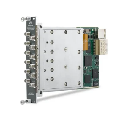
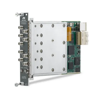
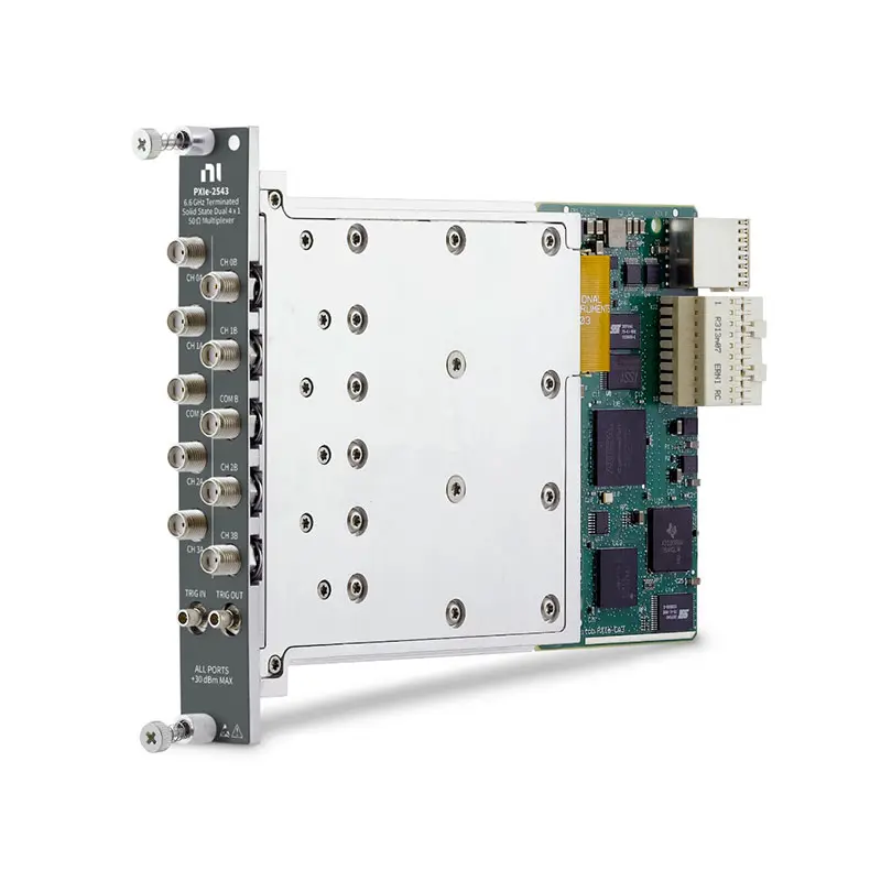
PXIe-2543 6.6 GHz Dual 4×1 RF Multiplexer Switch Module
Земля PXIe-2543 is a high-speed PXI Express RF multiplexer switch module designed for automated RF testing, signal routing and measurement-system integration. It provides two independent 4×1 multiplexers for connecting one of four RF channels to the corresponding common port in each bank.
The module uses solid-state FET switching technology to deliver a maximum switch operate time of 76 µs and effectively unlimited mechanical switching life. Its 50 Ω, AC-coupled architecture supports signals from 10 MHz to 6.6 GHz, while integrated termination on every channel and common line helps control reflections from unselected RF paths.
Key Features of the PXIe-2543
- Two independent 4×1 RF multiplexer banks
- Eight RF input channels and two common ports
- 10 MHz to 6.6 GHz frequency range
- 50 Ω nominal characteristic impedance
- AC-coupled signal paths
- 50 Ω termination on every channel and common line
- High-performance solid-state FET switches
- 76 µs maximum switch operate time
- Effectively unlimited mechanical relay life
- Less than 7.0 dB maximum insertion loss at 6.6 GHz
- Less than 6.1 dB typical insertion loss at 6.6 GHz
- Greater than 59 dB channel-to-common isolation at 6.6 GHz
- Less than −90 dB typical bank-to-bank crosstalk
- Less than 10 ps typical channel-to-channel skew
- +30 dBm maximum continuous RF input with chassis power on
- PXI and front-panel hardware trigger support
- Ten female SMA RF connectors
- Two female SMB trigger connectors
- PXI Express bus interface
- NI-SWITCH and NI Switch Executive support
PXIe-2543 Technical Specifications
| Product Model | PXIe-2543 |
|---|---|
| Part Number | 780587-43 |
| Product Type | PXI Express RF multiplexer switch module |
| Topology | Dual 4×1 terminated multiplexer |
| Number of Banks | 2 independent banks |
| Channels per Bank | 4 |
| Total RF Channels | 8 channels and 2 common ports |
| Minimum Input Frequency | 10 MHz |
| Максимальная частота | 6.6 GHz |
| Characteristic Impedance | 50 Ω nominal |
| Input Coupling | AC |
| Termination | 50 Ω termination on channels and common ports |
| Switch Type | Solid-state FET |
| Maximum Safe DC Input Voltage | ±8 V |
| Maximum Continuous RF Power, Chassis On | +30 dBm |
| Maximum Continuous RF Power, Chassis Off | +20 dBm |
| Insertion Loss at 2.4 GHz | Less than 4.1 dB, less than 3.4 dB typical |
| Insertion Loss at 6 GHz | Less than 5.8 dB, less than 5.1 dB typical |
| Insertion Loss at 6.6 GHz | Less than 7.0 dB, less than 6.1 dB typical |
| VSWR at 2.4 GHz | Less than 1.7, less than 1.5 typical |
| VSWR at 6 GHz | Less than 1.8, less than 1.5 typical |
| VSWR at 6.6 GHz | Less than 2.4, less than 1.6 typical |
| Channel-to-Common Isolation at 6.6 GHz | Greater than 59 dB, greater than 72 dB typical |
| Channel-to-Channel Isolation at 6.6 GHz | Greater than 53 dB, greater than 71 dB typical |
| Typical Bank-to-Bank Crosstalk | Less than −90 dB |
| Typical Channel-to-Channel Skew | Less than 10 ps |
| Typical Propagation Delay | 1,720 ps |
| Minimum Input 1 dB Compression | Greater than +27.6 dBm |
| Typical Input 1 dB Compression | Greater than +32.0 dBm |
| Typical Input IP2 | Greater than +89 dBm |
| Typical Input IP3 | Greater than +54 dBm |
| Maximum Switch Operate Time | 76 µs |
| Input Trigger Sources | PXI trigger lines 0 through 7 and front-panel trigger input |
| Minimum Trigger Pulse Width | 150 ns with digital filtering enabled |
| Output Trigger Destinations | PXI trigger lines 0 through 7 and front-panel trigger output |
| Output Trigger Pulse Width | Programmable from 1 µs to 62 µs |
| RF Connectors | 10 × female SMA jacks |
| Trigger Connectors | 2 × female SMB jacks |
| Шинный интерфейс | PXI Express |
| Module Format | 3U, one-slot PXI Express module |
| Dimensions | 21.6 × 2.0 × 13.0 cm |
| Weight | 774 g |
| Operating Temperature | 0°C to 55°C |
| Storage Temperature | −20°C to 70°C |
| Relative Humidity | 5% to 85%, noncondensing |
| Maximum Operating Altitude | 2,000 m |
| Поддержка программного обеспечения | NI-SWITCH and NI Switch Executive |
PXIe-2543 RF Performance
| Frequency | Maximum Insertion Loss | Maximum VSWR | Minimum CH-to-COM Isolation | Minimum CH-to-CH Isolation |
|---|---|---|---|---|
| Up to 2.4 GHz | 4.1 dB | 1.7 | 70 dB | 69 dB |
| До 6 ГГц | 5.8 dB | 1.8 | 61 dB | 58 dB |
| Up to 6.6 GHz | 7.0 dB | 2.4 | 59 dB | 53 dB |
PXIe-2543 Part Number and Accessories
| Item | Part Number | Описание |
|---|---|---|
| PXIe-2543 | 780587-43 | 6.6 GHz, 50 Ω, dual 4×1 terminated solid-state RF multiplexer |
| SMA Male-to-Male Cable | 763443-01 | 0.15 m, 50 Ω flexible SMA RF cable |
| SMA Male-to-Male Cable | 763444-01 | 0.45 m, 50 Ω flexible SMA RF cable |
| SMA 50 Ω Termination Plug | 778353-01 | Terminates unused external RF connections |
| RF Torque Screwdriver and SMA Driver Bit | 780895-01 | Tool set for tightening compatible SMA connectors |
| RF SMA Driver Bit | 780894-01 | Replacement SMA driver bit |
The PXIe-2543 provides direct front-panel RF connections and does not require a dedicated terminal block. Select cables and terminations according to the required frequency, insertion loss, flexibility and test-fixture layout.
Dual 4×1 RF Multiplexer Architecture
The PXIe-2543 contains two independent multiplexer banks identified as bank A and bank B. Each bank provides four channel connections and one common connection.
Software can connect CH0A, CH1A, CH2A or CH3A to COM A. The second bank independently connects CH0B, CH1B, CH2B or CH3B to COM B.
This architecture allows two RF instruments or two instrument ports to access separate groups of four test points. The banks can also be used together for two-port RF measurements.
Terminated RF Multiplexer Design
Every channel and common line includes a 50 Ω termination path. Unselected channels are routed to their corresponding terminations, helping reduce signal reflections and maintain predictable loading throughout an automated switching sequence.
Terminated architecture is particularly useful when connected RF sources or devices require a controlled 50 Ω load even when they are not selected by the multiplexer.
Power-On State
At power-on, the channel and common connections are routed to the module’s internal 50 Ω terminations. This provides a predictable initial state before the application creates an active channel-to-common route.
The complete system design should still account for chassis power loss. NI specifies a lower maximum continuous RF power of +20 dBm when chassis power is off, compared with +30 dBm when the chassis is powered.
10 MHz to 6.6 GHz Operation
The PXIe-2543 supports AC-coupled RF signals from 10 MHz through 6.6 GHz. This frequency coverage is suitable for wireless communications, RF component testing, aerospace electronics, automated receiver testing and general-purpose microwave routing.
The module does not provide a DC signal path. Applications requiring DC continuity or signals below 10 MHz should use a switch module with suitable DC-coupled specifications.
50 Ω Characteristic Impedance
The module uses a nominal 50 Ω architecture compatible with common RF signal generators, spectrum analyzers, vector network analyzers, RF digitizers and vector signal transceivers.
All connected cables, adapters and instruments should use 50 Ω interfaces. Connecting 75 Ω components can create impedance discontinuities, reflections and measurement errors.
Fast FET Switching
The PXIe-2543 uses FET switches instead of electromechanical relays. Maximum switch operate time is 76 µs, allowing signal routes to change much faster than many mechanical RF multiplexers.
Fast switching supports applications that must test many RF points in a short period, including production testing, multiband receiver validation and automated characterization.
Unlimited Mechanical Switching Life
FET switching eliminates the mechanical contacts used by conventional electromechanical relays. As a result, the PXIe-2543 does not have a finite mechanical relay-cycle rating under normal operation within its specified limits.
This characteristic makes the module useful for high-cycle applications that would consume the service life of an electromechanical multiplexer more quickly.
Insertion Loss
Maximum insertion loss is less than 4.1 dB at 2.4 GHz, less than 5.8 dB at 6 GHz and less than 7.0 dB at 6.6 GHz. Typical insertion loss at 6.6 GHz is less than 6.1 dB.
Solid-state switches generally introduce more insertion loss than comparable electromechanical RF relays. Test-system software can compensate for this predictable loss through path calibration or stored correction values.
Channel Isolation
Specified channel-to-common isolation remains greater than 59 dB at 6.6 GHz, while channel-to-channel isolation remains greater than 53 dB. Typical values are higher under the specified operating conditions.
High isolation helps reduce leakage from unselected sources and test points. Actual system isolation also depends on cable routing, connector condition, shielding and external fixture construction.
Low Bank-to-Bank Crosstalk
Typical crosstalk between the two multiplexer banks is less than −90 dB. This supports applications where bank A and bank B carry different signals or operate as separate paths in a two-port measurement system.
External cables should be routed carefully because coupling outside the module can reduce the overall isolation achieved by the test system.
Low Channel-to-Channel Skew
Typical channel-to-channel skew is less than 10 ps, while typical propagation delay is 1,720 ps. Consistent path timing is useful when comparing phase or timing-sensitive measurements across several RF channels.
External cable-length differences normally contribute more skew than the switch module. Use phase-matched cables when relative phase or delay accuracy is important.
RF Power Handling
With chassis power on, the maximum safe continuous RF input is +30 dBm. When chassis power is off, the maximum is reduced to +20 dBm.
These limits apply to safe continuous RF input and should not be interpreted as guaranteed linear operating levels. For applications requiring low distortion, consider the specified compression and intermodulation characteristics.
Compression and Linearity
The minimum input 1 dB compression point is greater than +27.6 dBm, with a typical value greater than +32.0 dBm. Typical input IP2 is greater than +89 dBm, and typical input IP3 is greater than +54 dBm.
These specifications help engineers estimate the distortion introduced when routing higher-level RF signals or multiple tones through the module.
Switching Active RF Signals
NI recommends against switching active RF signals. During a route change, the signal path is momentarily unterminated, and the resulting reflections can damage certain RF sources.
Disable or sufficiently reduce the source output before changing the selected channel. After the FET path and connected equipment have settled, restore the RF output and begin the measurement.
Automated Multi-Point RF Measurements
The PXIe-2543 allows one RF instrument to measure four test points in each bank without manual cable changes. Two banks provide independent routing for two instruments or two ports of a measurement system.
Automated switching improves test repeatability, reduces connection errors and allows software to execute the same routing sequence across multiple devices under test.
Vector Network Analyzer Integration
The dual-bank configuration can support switched two-port vector network analyzer measurements. One bank can route the analyzer’s source or port 1, while the other bank routes the return path or port 2.
Each path should be characterized or calibrated independently. Cable movement, connector repeatability and switch insertion loss can affect amplitude, phase and group-delay measurements.
Тестирование беспроводных устройств
The 6.6 GHz bandwidth supports many wireless communications and RF validation applications. Test software can connect transmitters, receivers, antennas or subsystem test points to shared RF instruments.
The terminated architecture helps maintain controlled loading on inactive paths, which can be important when testing RF devices that remain active during a multichannel sequence.
Production RF Testing
Fast solid-state switching makes the PXIe-2543 suitable for high-throughput production testing. The module can rapidly connect a signal generator or analyzer to multiple RF ports on a product or test fixture.
Because there are no mechanical relay contacts, frequent switching does not consume a conventional mechanical relay-cycle rating. This can reduce maintenance requirements in high-volume systems.
Hardware Triggering
The module can accept input triggers from PXI trigger lines 0 through 7 or the front-panel SMB trigger input. Output triggers can be routed to the PXI trigger lines or front-panel SMB output.
Hardware triggering allows route changes to be coordinated with RF sources, analyzers, digitizers and other PXI Express instruments. The programmable output-trigger pulse width ranges from 1 µs to 62 µs.
NI-SWITCH Software Support
The PXIe-2543 is controlled with the NI-SWITCH instrument driver. NI-SWITCH provides functions for initializing the module, connecting and disconnecting channels, creating scan lists, configuring triggers and monitoring module status.
The driver supports LabVIEW, LabWindows/CVI and compatible text-based development environments. It also includes a software front panel for interactive configuration and troubleshooting.
NI Switch Executive Integration
NI Switch Executive allows developers to define named routes instead of managing every physical channel identifier directly in application code.
Names such as RF input 1, calibration reference, VNA port 1 and DUT output can make automated test programs easier to understand and maintain. Switch Executive can also store route-related RF path-calibration information.
PXI Express System Integration
The PXIe-2543 occupies one slot in a compatible PXI Express chassis. It can be combined with RF signal generators, vector signal transceivers, spectrum analyzers, digitizers and other PXI modules to create a compact automated test platform.
Before installation, verify chassis slot compatibility, controller communication, cooling and the required NI-SWITCH software version. Power off the chassis before inserting or removing the module.
Typical PXIe-2543 Applications
- Automated RF signal routing
- Multi-point RF measurements
- Проверка беспроводных устройств
- Receiver and transmitter testing
- Vector network analyzer switching
- RF signal generator routing
- Spectrum analyzer input selection
- Two-port component characterization
- RF production testing
- Aerospace and defense electronics testing
- Research and laboratory automation
- High-cycle RF switch applications
PXIe-2543 Troubleshooting
The PXIe-2543 is not detected in NI MAX
Confirm that the module is fully installed in a compatible PXI Express slot. Check chassis power, controller communication and NI-SWITCH installation, then restart NI Measurement & Automation Explorer and rescan the system.
The common port has no RF signal
Verify that the correct bank and channel are selected. Check the SMA cables, source output, instrument input and software route configuration. Remember that the module is AC coupled and does not pass DC signals.
The signal level is lower than expected
Account for the PXIe-2543 insertion loss together with cable, adapter and fixture losses. At 6.6 GHz, the module’s specified insertion loss can be as high as 7.0 dB.
Measurements differ between channels
Characterize each route separately and store channel-specific correction values. Differences in cable length, connector condition, fixture routing and switch paths can affect amplitude and phase.
Reflections or VSWR are excessive
Confirm that all external devices use 50 Ω impedance and that unused external connections are terminated when required. Inspect SMA connectors and ensure that cables support the operating frequency.
The RF source reports a protection fault
Do not change routes while the RF source is active. Disable the output before switching because the path may be momentarily unterminated during a route change.
Hardware triggering does not work
Verify the selected PXI trigger line or front-panel SMB connection. Confirm the trigger polarity, minimum pulse width, digital-filter configuration and output-trigger pulse-width setting.
Switching is slower than expected
The specified 76 µs value describes switch operation under defined conditions. The complete test sequence may also require source muting, relay settling, instrument configuration and DUT stabilization time.
PXIe-2543 Comparison with Similar RF Multiplexers
| Модель | Конфигурация | Bandwidth and Switch Type | Best Suited For |
|---|---|---|---|
| PXIe-2543 | Dual 4×1, terminated | 6.6 GHz, FET | Fast, high-cycle, two-bank RF routing |
| PXIe-2544 | Single 8×1, terminated | 6.6 GHz, FET | Connecting one instrument to eight RF channels |
| PXI-2545 | Single 4×1, terminated | 2.7 GHz, electromechanical | Lower-loss terminated routing with fewer channels |
| PXI-2546 | Dual 4×1, unterminated | 2.7 GHz, electromechanical | Two-bank routing without internal terminations |
| PXI-2547 | Single 8×1, unterminated | 2.7 GHz, electromechanical | Eight-channel routing when termination is not required |
PXIe-2543 vs PXIe-2544
Both modules provide 6.6 GHz bandwidth, FET switching and terminated 50 Ω RF paths. The PXIe-2543 contains two independent 4×1 banks, while the PXIe-2544 provides a single 8×1 multiplexer.
Choose the PXIe-2543 when the application requires two independently controlled common ports or two-port measurements. Choose the PXIe-2544 when one RF instrument must access as many as eight channels.
PXIe-2543 vs PXI-2546
The PXIe-2543 and PXI-2546 both provide dual 4×1 multiplexer architectures. The PXIe-2543 uses terminated FET paths and supports frequencies through 6.6 GHz, while the PXI-2546 uses unterminated electromechanical relays and supports lower frequencies.
Select the PXIe-2543 for faster switching, higher switching-cycle requirements and controlled termination. Select the PXI-2546 when DC coupling, lower insertion loss or an unterminated path is more important.
FET vs Electromechanical RF Multiplexers
FET switches provide fast operation and no mechanical contact wear, making them suitable for high-throughput or high-cycle applications. Their tradeoffs can include higher insertion loss, AC coupling and lower maximum signal voltage.
Electromechanical RF relays generally provide DC continuity and lower path loss but switch more slowly and have a finite mechanical operating life.
Recommended Related Products
- PXIe-2544 6.6 GHz 8×1 RF Multiplexer Module
- PXI-2545 4×1 Terminated RF Multiplexer Module
- PXI-2546 Dual 4×1 RF Multiplexer Module
- PXI-2547 8×1 RF Multiplexer Module
- PXIe-2746 Four-Bank RF Multiplexer Module
- View More NI PXI and PXI Express Modules
Selecting the Right RF Multiplexer
Choose the PXIe-2543 when the test system requires two independent four-channel RF banks, operation through 6.6 GHz, integrated 50 Ω termination and fast solid-state switching.
Select the PXIe-2544 when one common port must connect to eight channels. Consider an electromechanical model when the application requires DC coupling, lower insertion loss or higher signal voltage instead of high switching speed.
Why Choose the PXIe-2543?
- Provides two independent 4×1 RF multiplexer banks
- Supports signals from 10 MHz to 6.6 GHz
- Uses high-speed solid-state FET switching
- Changes routes in as little as 76 µs
- Eliminates mechanical relay-cycle limitations
- Terminates channels and common ports at 50 Ω
- Provides strong channel and bank isolation
- Supports PXI and front-panel hardware triggers
- Occupies only one PXI Express chassis slot
- Integrates with NI-SWITCH and NI Switch Executive
Frequently Asked Questions
What is the PXIe-2543?
The PXIe-2543 is a 6.6 GHz, 50 Ω, dual 4×1 terminated PXI Express RF multiplexer switch module.
What is the PXIe-2543 part number?
The standard NI part number for the PXIe-2543 is 780587-43.
How many RF channels does it provide?
The module provides two independent banks, each containing four input channels and one common port. It therefore has eight RF channels and two common connections.
What is the supported frequency range?
The PXIe-2543 supports AC-coupled RF signals from 10 MHz through 6.6 GHz.
Does the PXIe-2543 pass DC signals?
No. Its signal paths are AC coupled, and the specified minimum input frequency is 10 MHz.
Does it terminate unselected channels?
Yes. The module includes 50 Ω termination on every channel and common line to help control reflections and maintain predictable RF loading.
What type of switches does it use?
The PXIe-2543 uses solid-state FET switches. This provides fast operation and eliminates mechanical contact-wear limitations.
What is the switching time?
The specified maximum switch operate time is 76 µs. Additional system settling time may be required depending on the source, instrument and DUT.
What is the maximum insertion loss?
Maximum insertion loss is less than 4.1 dB at 2.4 GHz, less than 5.8 dB at 6 GHz and less than 7.0 dB at 6.6 GHz.
What is the maximum RF input power?
Maximum safe continuous RF power is +30 dBm when the chassis is powered and +20 dBm when chassis power is off.
Which connectors does the PXIe-2543 use?
The module provides ten female SMA connectors for RF signals and two female SMB connectors for front-panel triggers.
Can it switch active RF signals?
NI recommends against changing routes while an active RF signal is applied because the path can be momentarily unterminated during switching.
Which software controls the PXIe-2543?
The module is controlled with NI-SWITCH and can be integrated with NI Switch Executive for named routes and RF path-calibration management.
Request a Quote for the PXIe-2543
Contact us for current availability, lead time and project pricing for the PXIe-2543 6.6 GHz Dual 4×1 RF Multiplexer Switch Module. We can also help identify compatible SMA cables, 50 Ω terminations, RF connector tools, PXI Express chassis and related NI RF switch modules for your automated test system.















